AMD's FPGA performance unit and GPU Chiplet patents tear the veil of the future
Source: IO Tech added 07th Jan 2021AMD’s Programmable Execution Unit (PEU) is intended to be placed in the processor core alongside existing integer and floating point units, and multi-chip GPU problems are to be solved with an interposer.
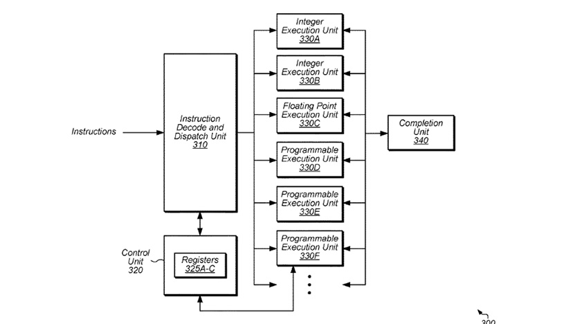
The first of AMD’s patents is closely related to the company’s recent acquisition of Xilinx. The “Method and apparatus for efficient programmable instructions in computer systems” patent describes in extremely simplified terms a programmable FPGA unit that would operate alongside the existing integer (INT) and floating point (FP) units and share the same registers with them.
According to the Reddit user marakeshmode analysis, the processors would have one or more PEUs (Programmable Execution Units) that can be programmed on the fly to suit the specific needs of each application. Multiple PEUs can also be programmed simultaneously for different needs, and programmability allows new and exotic computational accuracies and data formats to be utilized on a fast schedule. The processor instruction decoder and the transmitting unit automatically recognize the instructions for the PEU and route them to the correct execution units. When there are no special needs, PEUs can be programmed to compute traditional INT and FP commands alongside normal units.
Potentially, the new execution unit could significantly change the current programming model when, instead of optimizing the program for the processor, the processor could be optimized for the programs.
Radeon one half turn, the more “small chips” build on the GPU. Graphics circuits are one of the largest, if not the largest chip in modern computers, and as we know, circuit yields decrease very rapidly as the circuit size increases. Utilization of several smaller circuits, in turn, has problems due to the current programming model, which does not bend easily and efficiently to the tasks of several separate chips. There are also problems in implementing sufficiently fast and energy-efficient communication channels.
In AMD’s new patent, communication between chips is implemented through a passive communication network with a separate purpose-designed interposer. The configuration processor communicates only with the first chip of the GPU, which communicates with other chips through the connection network described above. Each chip has its own private L2 cache, which is connected between the Infinity Fabric (Scalable Data Fabric) to the inter-chip communication bus and further to the common, all-chip coherent L3 cache found on each chip. The L3 caches are connected to the memory controllers found on each chip.
Sources: FreePatentsOnline (1), (2), Reddit
brands: AMD Fly Infinity New other Unit XILINX media: IO Tech keywords: Memory Radeon
Related posts
Notice: Undefined variable: all_related in /var/www/vhosts/rondea.com/httpdocs/wp-content/themes/rondea-2-0/single-article.php on line 88
Notice: Undefined variable: all_related in /var/www/vhosts/rondea.com/httpdocs/wp-content/themes/rondea-2-0/single-article.php on line 88
Related Products
Notice: Undefined variable: all_related in /var/www/vhosts/rondea.com/httpdocs/wp-content/themes/rondea-2-0/single-article.php on line 91
Warning: Invalid argument supplied for foreach() in /var/www/vhosts/rondea.com/httpdocs/wp-content/themes/rondea-2-0/single-article.php on line 91
