Scientists at the University of Massachusetts Amherst have introduced a novel method for aligning layers in chips using lasers and metalenses. The new technique is claimed to achieve accuracy down to the atomic scale, reports SciTechDaily. This advancement could be critical for next generation process technologies as well as integration of multi-chiplet 3D designs.
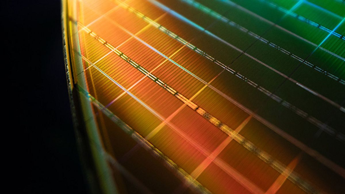
Overlay accuracy — precise alignment of one layer of a chip with the underlying layer — is one of the most critical capabilities of today’s chipmaking tools as each wafer with logic chips requires over 4,000 manufacturing steps performed by different machines. Contemporary chipmaking tools perform overlay operations primarily using advanced optical metrology, alignment marks, and closed-loop control systems integrated into photolithography systems.
However, existing methods face limitations such as the inability to simultaneously focus on widely spaced layers and a resolution limit of about 2 – 2.5nm. These issues introduce potential inaccuracies during refocusing and positioning, which could be problematic for both for next-gen production nodes and vertically stacked multi-chiplet designs in the future.
The method proposed by the UMass Amherst team involves placing specially designed concentric metalenses on chip surfaces. When illuminated with a laser, these lenses generate holographic interference patterns. By analyzing these patterns, researchers can determine how much two chip layers are misaligned, including the direction and precise amount of displacement across all three spatial axes.
Their technique can detect lateral misalignments as small as 0.017nm and vertical deviations down to 0.134nm. This surpasses their original goal of 100nm precision and exceeds what optical microscopes can resolve. Furthermore, they believe that the method could lower manufacturing costs by simplifying one of the most complex steps in chip production and 3D chip integration. Unfortunately, it is unclear whether the setup can be integrated with existing lithography tools, bonding tools, and though silicon vias formation tools. If not, the technology will hardly gain grounds in the semiconductor industry.
This laser hologram technology has implications beyond chip manufacturing. A similar setup — a basic laser source and a camera — can be adapted to measure physical movements. For instance, a shift in a surface due to pressure or vibration can be translated into an optical signal. This opens opportunities in applications like environmental sensing, industrial monitoring, and biomedical diagnostics.