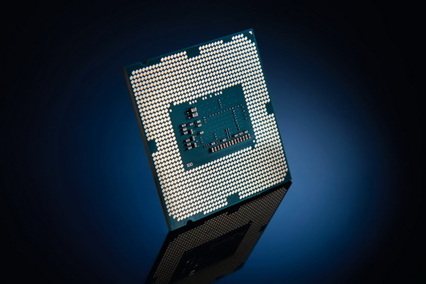
CES 2021: Intel Rocket Lake-S processor die details revealed
Source: Geeknetic added 14th Jan 2021During this virtual version of CES 2021 we have been able to see a large amount of new hardware, either in the face of separate components or finished products, and among them we can find the new Intel Rocket Lake-S processors. At the presentation event, several details were revealed, including a real color image of the die of the Intel Rocket Lake-S, and thanks to @Locuza_ on Twitter, now we can see in detail what each part corresponds to.
To begin with, we can see how practically half the area of the die of Rocket Lake-S is taken by the Uncore and the iGPU, while the rest is the one dedicated to the Cypress Cove cores, that we remember, they are supposed to be a back -port of Willow Cove to 14 nanometers, although some changes.
Each Cypress Cove core has 512 kB of L2 cache, in addition to counting co n an L3 cache of 16 MB divided into 2MB parts that is fully accessible by any kernel of the processor. The L1 caches remain identical to the Willow Cove cores.
On the other hand, the iGPU of the processor is the Intel Gen 12 Xe-LP GT1, being the GPU Intel’s smallest for this generation with a total of 32 execution units providing a total of 256 cores, well below the 96 execution units of the GT2 version of the same GPU. Still Intel says that this GPU is a 50 percent more powerful than the Intel Gen9.5 GT2 found in Comet Lake -S.
Finally, we find Uncore, which has grown to accommodate the necessary architecture for PCI Express 4.0, which also grows to a total of 28 PCI Express lanes.
End of Article. Tell us something in the Comments or come to our Forum!
