For tomorrow's technology: from quantum dots to quantum technologies
Source: Heise.de added 28th Dec 2020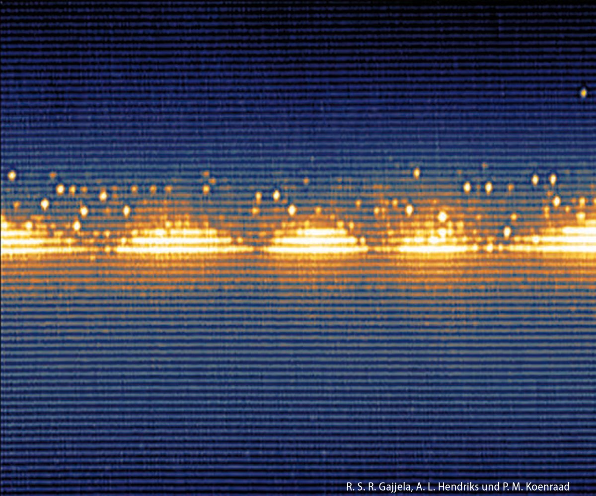
The properties of electronically zero-dimensional quantum dots in semiconductor heterostructures differ fundamentally from those in higher-dimensional structures such as quantum wells. In quantum dots, the energy of charge carriers is not a function of the momentum. Their properties are similar to those of atoms embedded in a dielectric matrix. Based on gas phase or molecular beam epitaxy, photonic and electronic components have been developed in recent years that enable completely new applications. This includes quantum cryptography, new types of non-volatile memory and an energy-efficient, high-bit-rate Internet.
The age of the information society from the middle of the 19. Century began with the development of silicon-based compounds and technologies. The manufacture of integrated electronic circuits (SiICs) began about 60 years ago. Their first commercial applications were hearing aids. Today silicon-based integrated circuits are part of almost all everyday objects and the basis of the information society.
Dieter Bimberg studied mathematics, philosophy and physics in Tübingen and Frankfurt am Main, where he received his doctorate in physics. For the Max Planck Society he dismantled 1972 the high-field magnet laboratory in Grenoble, where he established a working group for optical spectroscopy headed. 1979 he accepted a position at RWTH Aachen. 1981 he followed the request of the TU Berlin to set up the Applied Physics course, where he 21 was Managing Director of the Institute for Solid State Physics and founder of the Center for Nanophotonics. Guest stays have taken him to the Technion in Haifa, the Royal Signals and Radar Establishment in Malvern (UK), the HP Labs in Palo Alto, the University of California in Santa Barbara and the King Abdulaziz University in Jeddah (Saudi Arabia). Since 2018 he has headed a new center for “Green Photonics” of the Chinese Academy of Sciences in Changchun. He is a member or Foreign Fellow of the German, Russian and American Academies of Sciences.
Procedures such as molecular beam epitaxy (MBE) or gas phase epitaxy ( MOCVD) for the production of materials whose expansion is only a few nanometers in all three spatial dimensions, ie of “zero-dimensional” quantum dots, and their embedding in other materials, open up completely new possibilities for using quantum mechanical effects today. The aim is to change the electronic and thus also optical and electrical properties of complex structures in a targeted manner. These properties depend on the shape and size of the quantum dots. Their expansion in all three spatial directions should be below the De Broglie wavelength of the charge carriers so that quantum mechanics dominates. Quantum dots enable new types of electronic and photonic components. Three examples of this, based on one, a few and very many quantum dots, are described below.
This article was first printed in Physik Journal 8/9, 2020.
Self-organization of quantum dots The discovery of new physical effects in the simplest, low-dimensional semiconductor structures – two-dimensional quantum wells – and their use for semiconductor lasers can be traced back to the work of two physicists at Bell Labs. Ray Dingle and Charles Henry 1972 filed a patent on quantum well lasers. In doing so, they described the advantages of reduced dimensionality among other things as a reduced threshold current density at which the laser emission begins. They showed how the density of states of electrons changes with the transition from three to two and finally one-dimensional structures. These changes are considered to be the determining factor for all properties of the material and its components.
It was not until much later that two Japanese groups at the University of Tokyo and the Tokyo Institute of Technology ( TIT) zero-dimensional structures. The group around Suematsu at TIT calculated 1981 that the material gain was increased by a factor 20 increases and the threshold current density decreases for quantum dot-based lasers that are based on InP or GaAs-based heterostructures. These theoretical considerations were based on heterostructures whose different layers have identical lattice constants. Thirty years ago, this was a prerequisite for defect-free structures and is still part of the technology of many photonic components today. In the eight years that followed, tremendous efforts were made to demonstrate the benefits of such quantum dot-based lasers. Based on the technologies used at the time, this did not succeed for various reasons, whereupon the international activities quickly subsided.
Self-organized growth as a key Surface physicists classify the growth modes for the coherent growth of one material on a second material into three groups. In the case of identical lattice constants, for example AlGaAs on GaAs, there is often a two-dimensional growth monolayer on monolayer – with steps and roughness. With different lattice constants, three-dimensional clusters can grow coherently. Alternatively, in the case of structures with different lattice constants in the Stranski-Krastanov growth mode, a wetting layer (also rough) and a few monolayers thick can first arise on which three-dimensional clusters then grow. The theoretical description of this growth is complex, since there are both lattice constant mismatches with the elastically anisotropic growth surface and edge-induced stresses. In addition, the tensions change the surface reconstruction and cause a renormalization of the surface energies of the islands and the wetting layer. Kinetic effects are important for the dynamics of growth at real temperatures.
The self-organization on strained surfaces, which was first identified experimentally in my work group and then theoretically confirmed, assumes that atoms are sufficiently mobile on the surface, which is the case at the typical growth temperatures of the quantum dots of a few hundred degrees.
Images with the transmission electron microscope (TEM) of a single layer of (InGa) As / GaAs quantum dots show the theoretically predicted pyramid structure. The quantum dots similar to each other are arranged in a square pattern. The edges of the base point along the – and [010] – directions, since all III-V connections have an elastically anisotropic (001) – own surface. We have demonstrated a pyramid shape of the quantum dots in a single layer for both MOCVD and MBE growth of (InGa) As / GaAs quantum dots using cross-sectional TEM and tunnel spectroscopy. The shape determines the electronic properties.
Cross-sectional TEM images of stacked quantum dot layers show that the quantum dots in the layers are arranged on top of one another completely free of defects due to the long-range elastic tension to let. This is of the utmost importance for the most diverse variants of quantum dot-based diode lasers, which are to be grown electronically coupled or uncoupled depending on the application. The superior material gain of a single layer can be converted into a modal gain that is greater than the losses due to the defect-free stacking. This explains the lowest density of the threshold current found by us of all diode lasers and the otherwise unmatched efficiency in converting electrical into optical energy.
The stress-induced self-organized growth of quantum dots is universal. GaN-based lasers, which emit in the visible, have quantum dots as active layers. Exotic examples are the little researched InAs / Si quantum dots for silicon photonics or GaSb quantum dots on (AlGa) P with GaAs interlayers for novel nanoflash memories, which are described below. In the case of a GaSb / GaAs / GaP quantum dot that was produced by means of gas phase epitaxy, adjacent surfaces of the quantum dot pyramids are inequivalent to one another (see title picture). This is of decisive importance for the electronic properties discussed in the next section: Quantum dots of four-fold pyramidal shape do not have a four-fold, but only a twofold symmetry of the electronic properties.
brands: AIM AM Century Charge Diverse HP Matrix Mobile New other Pyramid Quantum Royal Silicon media: Heise.de keywords: Internet Memory Mobile
Related posts
Notice: Undefined variable: all_related in /var/www/vhosts/rondea.com/httpdocs/wp-content/themes/rondea-2-0/single-article.php on line 88
Notice: Undefined variable: all_related in /var/www/vhosts/rondea.com/httpdocs/wp-content/themes/rondea-2-0/single-article.php on line 88
Related Products
Notice: Undefined variable: all_related in /var/www/vhosts/rondea.com/httpdocs/wp-content/themes/rondea-2-0/single-article.php on line 91
Warning: Invalid argument supplied for foreach() in /var/www/vhosts/rondea.com/httpdocs/wp-content/themes/rondea-2-0/single-article.php on line 91