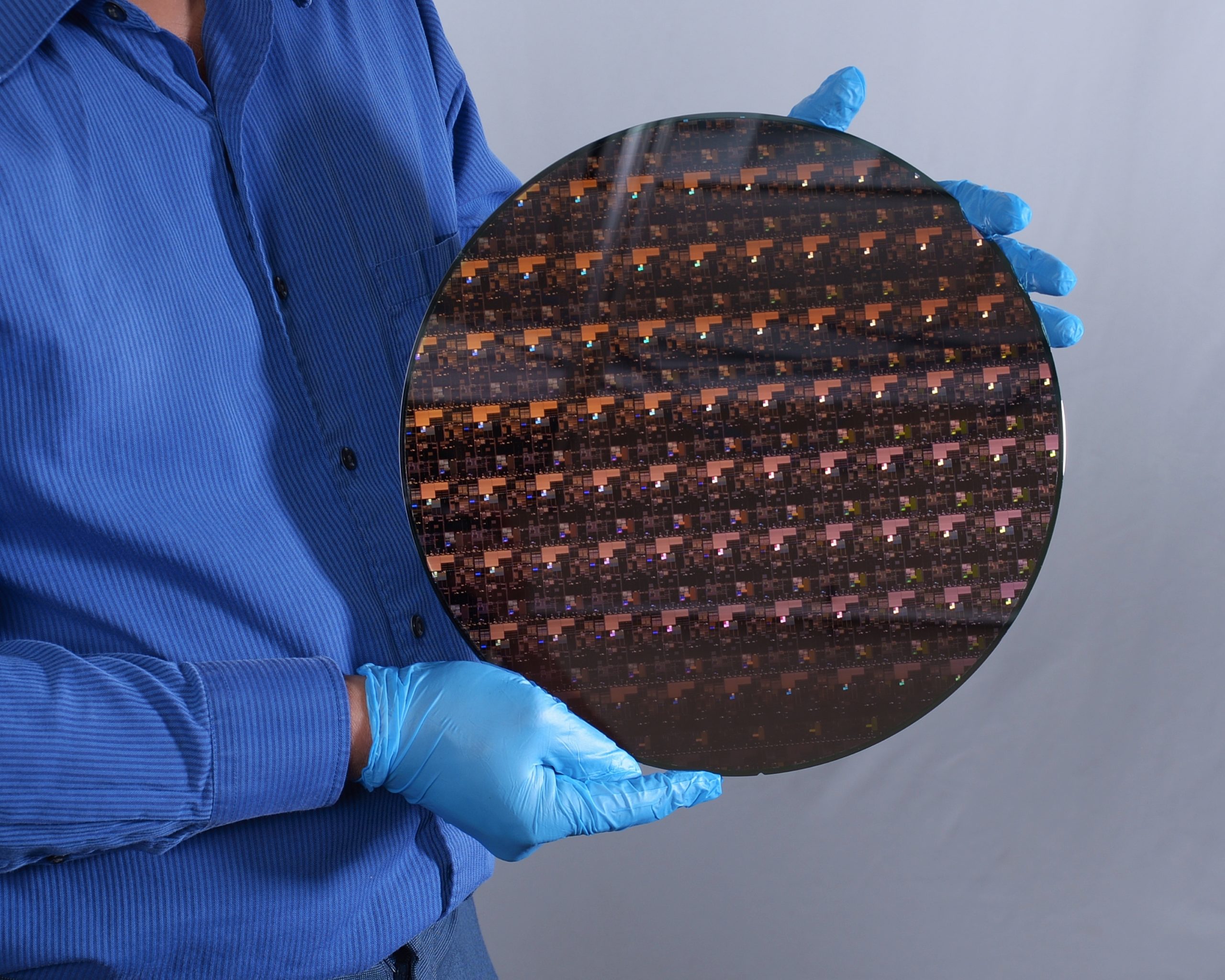
IBM research unveiled a new 2nm chip with nanosheet technology today that will serve as the underpinning of its future process technology. IBM displayed a full 300mm wafer produced on the 2nm nanosheet process at its Albany, New York facilities. However, it is important to remember that the technology is still in the research phase, so the wafer doesn’t have productizable chips, at least in their current form.
IBM no longer mass-produces processors; instead, it helps develop technology for its partners, like Intel and Samsung. The former recently announced that it would research new process node and packaging technologies with IBM as part of its new IDM 2.0 initiative. That means that Intel’s future 2nm chips could be based on some of these IBM breakthroughs, and there are plenty.
IBM claims that the new process node tech will improve performance by 45% using the same amount of power or 75% less power while maintaining the same performance as today’s 7nm processes.
IBM says the new chips will feature up to 50 billion transistors in a chip the ‘size of a fingernail’ but hasn’t provided transistor density metrics (MTr/mm2) that would give us a better sense of how density compares to other modern chips.
However, as with all modern chip node naming conventions, it’s important to remember that the ‘2nm’ metric isn’t tied to a specific physical feature on the chip. Instead, it’s developed based on the power consumption and performance of comparable process nodes from third-party foundries, meaning that modern chip nanometer naming is largely a marketing exercise. That’s an industry-wide problem that isn’t confined to IBM, though.
Image 1 of 4
Image 2 of 4
Image 3 of 4
Image 4 of 4
The first image in the album above shows a cross-section of six of IBM’s 2nm transistors. If you’re accustomed to looking at electron microscope cross-sections of transistors, you’ll notice these are markedly different from the third image, which is Intel’s current-gen 14nm FinFET technology.
IBM’s new design consists of three stacked horizontal silicon nanosheets, with each nanosheet surrounded entirely by a gate. This ‘gate-all-around’ (GAA) technique reduces voltage leakage that prevents switching off the transistors. This is becoming more of an issue as transistors shrink — even when the gate surrounds the channel on three sides, as we see with FinFET transistors (illustrated in the final image).
Image 1 of 2
Image 2 of 2
Here we can see IBM’s slides on its 2nm nanosheet transistors and the various measurements. Each transistor has three stacked nanosheet layers surrounded by gates, and the entire stack measures 75nm tall in aggregate. Each nanosheet measures 5nm x 40nm with a 12nm gate length, and the transistor has a 44nm pitch.
IBM has made several other notable steps forward with the tech, including the industry-first Bottom Dielectric Isolation to eliminate leakage current from the first nanosheet in the stack, enabling the 12nm gate length. IBM isn’t sharing further details on the materials it uses in the 2nm process, such as if it uses silicon-germanium, but the company says it will share more details in the future.
IBM’s 2nm process is also the first to use EUV lithography on the front-end-of-line (FEOL) portion of the chip where the transistors and associated structures are created (nanosheets and gate). In contrast, currently-shipping transistor technology uses EUV patterning in the middle-of-line (MOL) and back-end-of-line (BEOL) stages that comprise the interconnects and packaging portions of the chip, respectively.
Surprisingly, IBM says that it uses single-exposure EUV in every critical layer of the chip, including FEOL, reducing complexity (fewer optical masks and steps) and improving yields compared to multi-patterning. This technique can create nanosheet widths from 15nm to 70nm, giving the fabs some flexibility with cell libraries and SRAMs based on various design targets. IBM also disclosed that it uses the Twinscan NXE:3400B EUV machine from ASML to produce its 2nm test wafers.
IBM ran its own chip-producing facilities for roughly 25 years before selling that portion of its business to GlobalFoundries back in 2014. However, IBM has continued its own research and development and licensing of its core technologies through its $3 billion ‘Seven Nanometers and Beyond’ research program that the company began after it sold its fabrication facilities. Samsung has been the company’s key partner, a relationship that will continue in the future with IBM’s process technology. In fact, Samsung will produce IBM’s own Power10 processors this year on a 7nm process developed in conjunction with IBM.
Intel’s announcement that it will collaborate with IBM on future logic and packaging technologies came as an understated overly-broad statement in its IDM 2.0 announcement a little over a month ago. However, the partnership holds momentous importance for Intel as it looks to recover from years of stagnation with its process technologies, and IBM was quite clear in our briefing that its new 2nm tech will benefit all of its partners, which includes Intel.
IBM has only shared the basic details of its 2nm nanosheet design, so there’s still much to learn, such as how the company plans to tackle interconnect scaling, which has become a key hurdle in the path to smaller transistors. Simply put, the smallest transistors in the world are of no use if you can’t wire them together, and that has been one of the most pressing constraints to shrinking to smaller nodes.
Additionally, IBM hasn’t shared details around SRAM, density metrics for the various cell libraries, or the materials it uses for the 2nm node. We expect all these questions, and hopefully more, to be answered as we worm our way to the first products based on the tech. IBM says it expects its 2nm nanosheet process to roll out of partner foundries in late 2024, but it didn’t give any firm projections which foundries would lead the way with tech based on its research.
