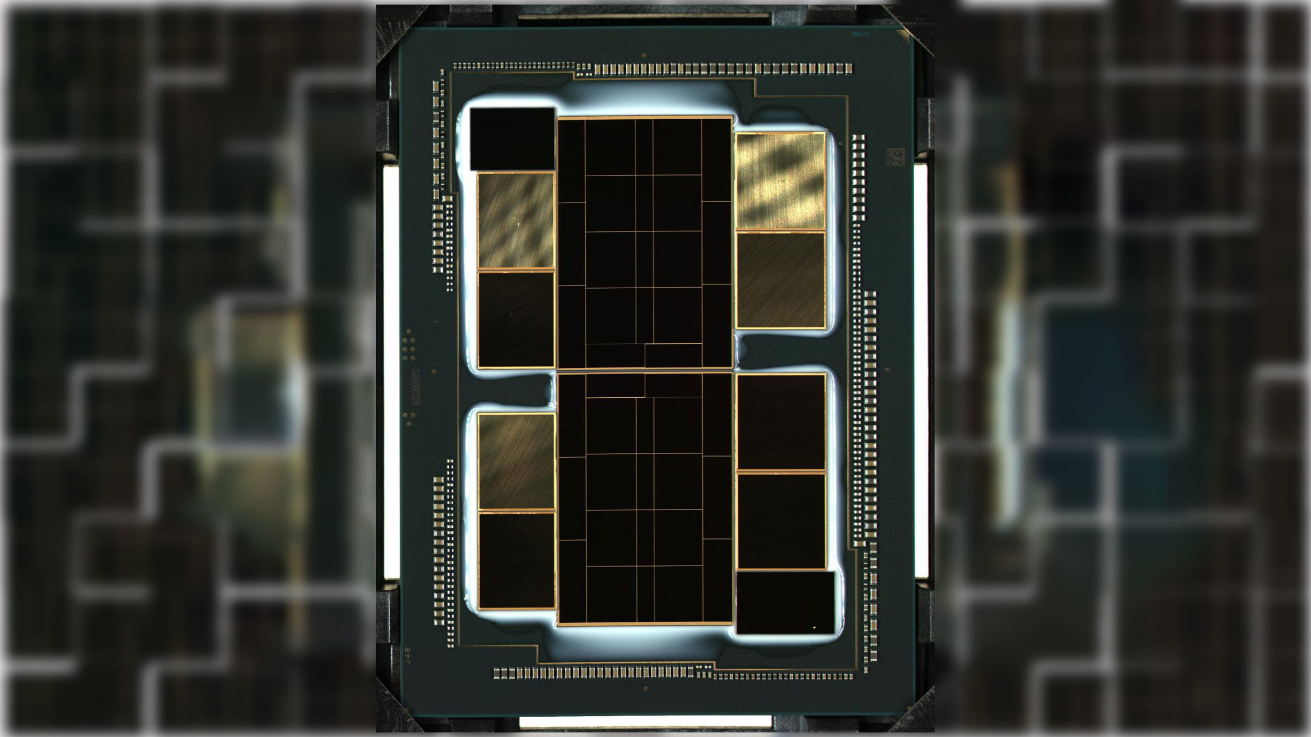
We’ve known about Intel Xe Graphics for ages, and the integrated Xe LP variant has been shipping in Tiger Lake laptops since last fall. Raja Koduri, Intel’s senior VP of Architecture, Graphics, and Software, has tweeted various images of Xe HP chips in the past. Today, he posted a die shot of the upcoming Xe HPC version, presumably meaning 7nm Ponte Vecchio. Specs are sort of unknown, though we have plenty of clues about what the final product will have in terms of specs.
The above image is the dual-chiplet variant, with the two halves connected via EMIB (Embedded Multi-die Interconnect Bridge). Around the outside of the two main GPU blocks are a bunch of supporting chips, and that’s where things get interesting. The rectangles aren’t all the same size, and there are five chips for each GPU. What are these chips, and what are the specs for each? It’s hard to say.
Raja mentions “7 advanced silicon technologies in a single package.” Some of these are easier to guess at than others; Foveros, EMIB, SuperFIN, Rambo Cache, HBM, and Compute Tiles have all been mentioned as being part of Xe HP. That’s six items, so we’re missing one, and it’s entirely possible Raja’s list is slightly different.
The two chips are inverted versions of each other in the die shot, mostly, but the blocks on the right are more square-shaped (200×216 pixels) than the blocks on the left (174×216 pixels). Then we have the top-left chip (186×138 pixels) and the bottom-right chip (218×138 pixels). Perhaps Intel is doing some creative image editing to obscure the chip dimensions, but then why post the image in the first place?
We do know that Intel is using its Foveros 3D chip stacking technology with Ponte Vecchio. Given the asymmetrical chip sizes, there are probably three different chips that contain one or more of the “tiles” that Intel has previously mentioned. Each chip could contain one or more of: HBM2, Rambo Cache, or Compute. But right now, we don’t know how Intel is distributing things.
As for the main GPU block, the die is blacked out, but we have a decent idea of what to expect, and the blocked out sections are easier to guess at. The center strip of four rectangles on each GPU is probably the fabric for routing data between the execution units. To the left and right of the center are eight identically sized blocks that likely each contain 64 EUs (Execution Units), with eight ALUs (aka, GPU cores) per EU. That gives 512 EUs per chip, and 1024 EUs for the entire package, with potentially 8196 “cores” if we’re trying to compare things with AMD and Nvidia GPUs.
The remaining six rectangles on the left and right sides are likely for memory and other interfaces to the HBM, Rambo Cache, and Compute tiles — or maybe just memory interfaces. Six memory controllers suggest a potential 6144-bit interface. That’s the same overall bus width as Nvidia’s A100, though Nvidia allows for one disabled interface and HBM2 chip per package. There are two smaller rectangles near where the two dies connect.
Even though we can’t say for certain what each of the blocks is doing, it’s clear that Intel has packed a lot of compute power into a single package. Previously, Raja showed off this package shot of Xe HP with a AA battery for scale. Whether that’s the same package we see in today’s die shot isn’t certain, but it seems likely. What any of this means for the consumer-focused Xe HPG, aka DG2, is anyone’s guess.
