Intel pulled the covers back on its Lunar Lake architecture during its Intel Tech Tour 2024, delivering deep dive architectural details in Taipei, Taiwan in advance of the company’s Computex 2024 keynote as its newest chips race to a Q3 launch. Intel’s Lunar Lake will have significant improvements in every facet of its design. Lunar Lake will primarily target mobile designs, powering some of the best laptops, though many of the fundamental changes will likely carry over to Arrow Lake and will be in some of the best CPUs for gaming.
Every component of the Lunar Lake architecture has been optimized for a refined blend of power and performance that intel says will redefine what we expect from x86 PCs. Some of the biggest improvements come in the E-cores, with 38% and 68% IPC gains in the new Skymont architecture. There’s also a 14% IPC gain for the Lion Cove P-cores — though these projections come with caveats. Graphics will see a 50% improvement in iGPU performance with the new Xe2 integrated graphics engine.
Lunar Lake incorporates Intel’s new neural processing unit (NPU) for AI workloads that delivers 48 TOPS of performance, easily providing enough performance to satisfy Microsoft’s requirement of 40 NPU TOPS for next-gen AI PCs. In fact, the Lunar Lake platform has far more AI performance under the hood — in total, it offers 120 TOPS when factoring in the CPU and iGPU.
The resulting Lunar Lake mobile chips employ an entirely new design methodology that focuses on ensuring power efficiency as a first-order priority, and this base architecture will be used as the building block for Intel’s future products, like Arrow Lake and Panther Lake. This new design focus is key to fending off a bevy of strong competitors in the laptop market from AMD, Apple, and now Qualcomm.
Surprisingly, intel turned to TSMC for its leading-edge 3nm N3B process node for its compute tile, which houses the CPU, GPU and NPU. It also uses the TSMC N6 node for the platform controller tile that houses the external I/O interfaces. In fact, the only Intel-fabbed silicon on the chip is the passive 22FFL Foveros base tile that facilitates communication between the tiles and the host system.
Intel says it chose TSMC’s nodes because they were the best available when the company began designing the chip, a nod to its delays on the manufacturing side of the operation as it looks to regain its lead in foundry technology through its five nodes in four years initiative. However, Intel designed the architectures to be easily portable to other process nodes, so we can expect it to return to using its own nodes with many of these same architectures in its future products.
Lunar Lake’s new microarchitectures pave the way for the company’s soon-to-be-announced Arrow Lake processors for the desktop, and even its Xeon 6 lineup, too. Let’s dive into the details.
Lunar Lake SoC Overview
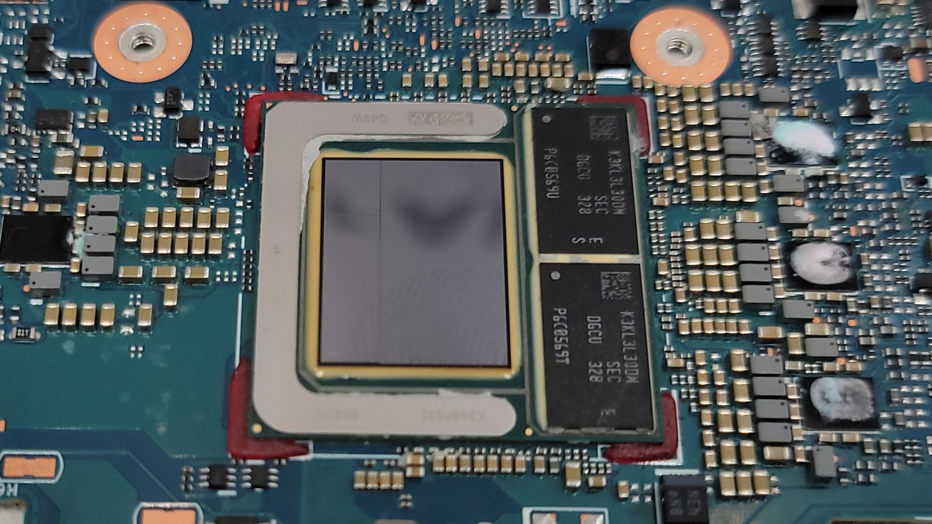
Intel’s Lunar Lake will come with four P-cores and four E-cores in the top-tier SKU. The chip is comprised of two logic tiles, a TSMC N3B compute tile and an N6 platform controller tile, along with a stiffener (a non-functional piece of filler silicon) placed atop a 22FFL base Foveros tile. The logic tiles are connected to the base tile with solder bonding with a 25-micron bump pitch (a critical measurement of interconnect density), an improvement over the 36-micron pitch used for Meteor Lake. This smaller pitch enables denser communication pathways between the units and helps reduce power consumption.
Intel places two stacks of LPDDR5X memory directly on the chip package, in 16GB or 32GB configurations, to reduce latency and board area while lowering the memory PHY’s power consumption by up to 40%. The memory communicates over four 16-bit channels and delivers up to 8.5 GT/s of throughput per chip.
The compute tile houses the CPU P- and E-cores, Xe2 GPU, and NPU 4.0. It also incorporates a new 8MB ‘side cache’ that can be shared among all the various compute units to improve hit rates and reduce data movement, thus saving power. However, it doesn’t technically fit the definition of an L4 cache because it is shared between all of the units.
Intel has also moved the power delivery subsystem from the chip to the board, with four PMICs spread across the motherboard to provide multiple power rails and increased control. Overall, Intel claims a 40% reduction in SoC power over Meteor Lake.
Let’s dive into the core microarchitecture for the CPU, GPU and NPU, along with details about the platform controller tile, on the following pages.