Intel uploaded a detailed description of its upcoming Ponte Vecchio Xe-HPC GPU for supercomputers just hours after outlining its IDM 2.0 strategy that involves usage of internal and external manufacturing capabilities. Ponte Vecchio, which employs components produced by Intel, Samsung, and TSMC using a variety of process technologies, demonstrates Intel’s vision of the future in the best way possible.
Intel’s codenamed Ponte Vecchio is the company’s first GPU based on the Xe-HPC microarchitecture that will be initially used for Argonne National Laboratory’s Aurora supercomputer along with Intel’s next-generation Xeon Scalable ‘Sapphire Rapids’ processor. The machine will be one of the industry’s first supercomputers to feature over 1 ExaFLOPS FP64 performance.
Over time, the part will be available to other customers and Intel might even customize it as it is relatively easy to do given the fact that the Ponte Vecchio uses a disaggregated modular architecture, Intel’s new approach to complex processors.
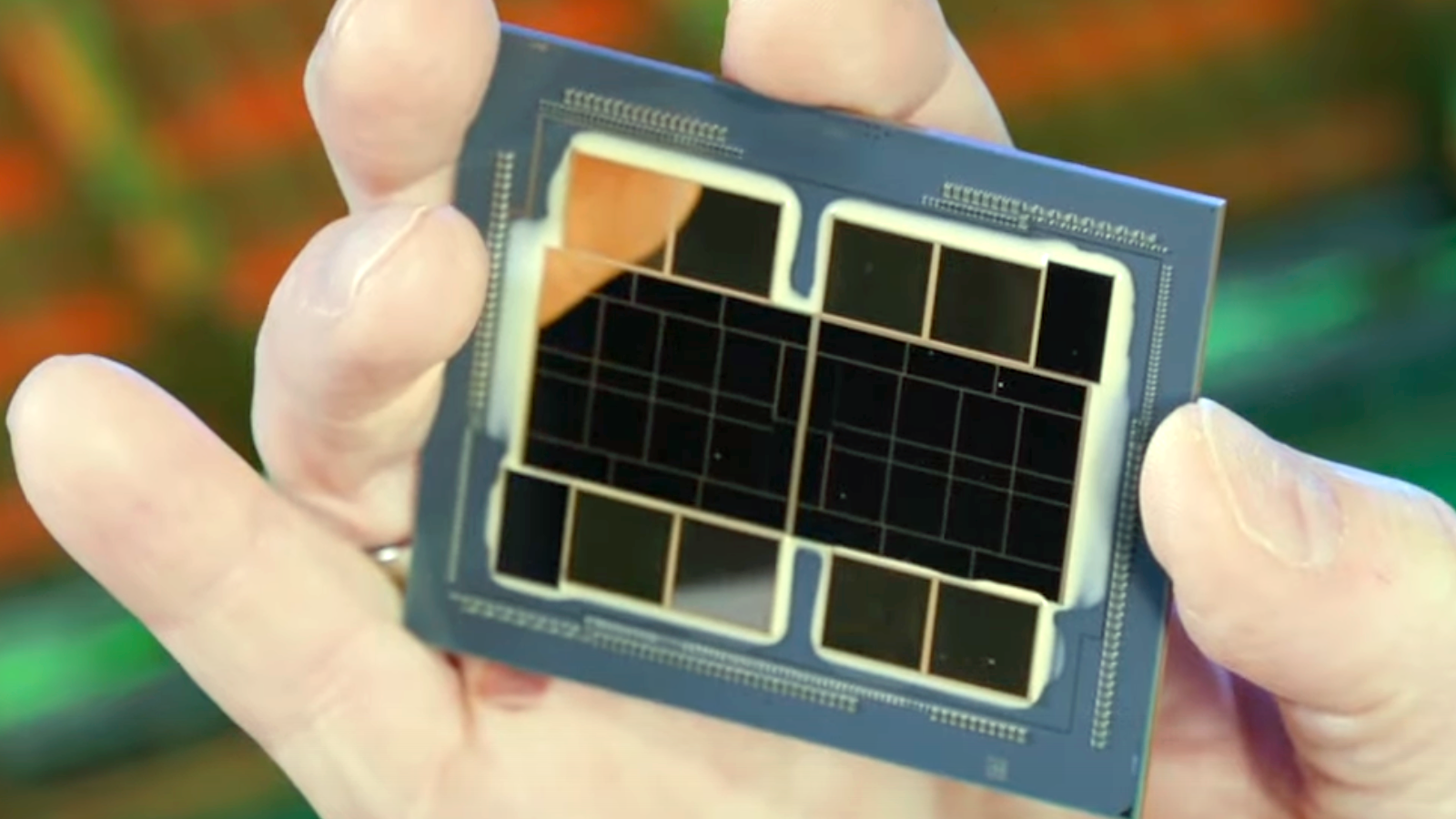
In fact, it would be impossible to build a monolithic Ponte Vecchio as it is a massive processor featuring 47 components, over 100 billion transistors, and offering PetaFLOPS-class AI performance (more on this later).
The Ponte Vecchio includes the following tiles/chiplets:
- 2 base tiles made using Intel’s 10 nm SuperFin technology
- 16 compute tiles produced by TSMC initially and then by Intel when its 7 nm technology is ready for high-volume manufacturing (HVM).
- 8 Rambo cache tiles fabbed using Intel’s 10 nm Enhanced SuperFin process
- 11 EMIB links made by Intel
- 2 Xe Link I/O tiles made by a foundry
- 8 HBM memory stacks produced by a DRAM manufacturer
At present, Intel only using its Ponte Vecchio Xe-HPC GPUs in the lab. While the modular design of the device allows the company to build it more or less cost efficiently, tailoring the design’s thermals, voltages, and frequencies is tricky and will take some time.
One interesting thing to note about Intel’s Ponte Vecchio description is that the chipmaker said that it offers ‘PetaFLOPS-class AI performance.’ There are numerous AI workloads that require different compute precision.
Intel usually considers FP16 to be the optimal precision for AI, so when the company says that that its Ponte Vecchio is a ‘PetaFLOP scale AI computer in the palm of the hand,’ this might mean that that the GPU features about 1 PFLOPS FP16 performance, or 1,000 TFLOPS FP16 performance. To put the number into context, Nvidia’s A100 compute GPU provides about 312 TFLOPS FP16 performance.
Argonne National Laboratory’s Aurora supercomputer is due in 2022.