Samsung introduced the first mass-produced 3D NAND memory, dubbed V-NAND, in 2013, well ahead of its rivals. Samsung started with 24-layer V-NAND chips back then, and now having gained plenty of experience with multi-layer flash memory, it is on track to introduce 176-Layer V-NAND devices. But that’s only the beginning —Samsung says it envisions V-NAND chips with more than 1,000 layers in the future.
176-Layer V NAND on Track for This Year, PCIe 5.0 Coming
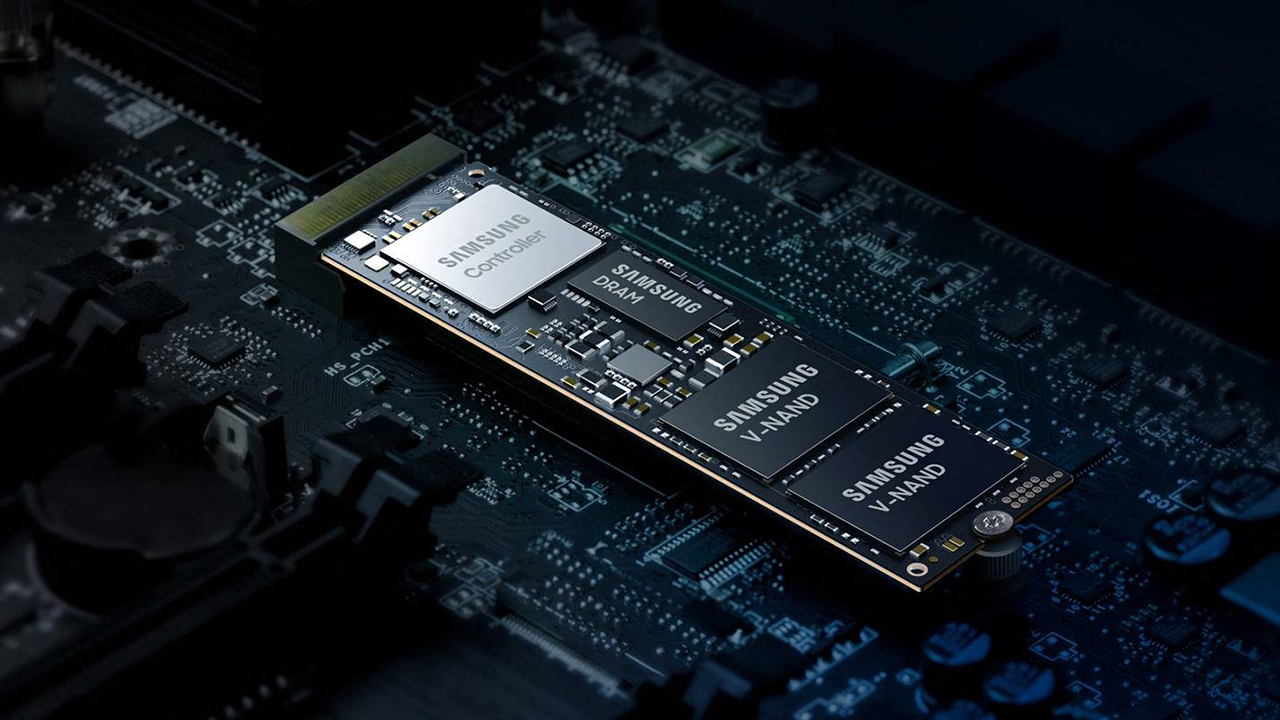
Samsung intends to begin producing consumer SSDs powered by its seventh-gen V-NAND memory that features 176 layers and, according to the company, the industry’s smallest NAND memory cells. This new flash’s interface boasts a 2000 MT/s data transfer rate, allowing Samsung to build ultra-fast SSDs with PCIe 4.0 and PCIe 5.0 interfaces. The drives will use an all-new controller ‘optimized for multitasking huge workloads,’ so expect a 980 Pro successor that demonstrates strong performance in workstation applications.
Over time, Samsung will introduce data center-grade SSDs based on its 176-Layer V-NAND memory. It’s logical to expect the new drives to feature enhanced performance and higher capacities.
First 200+ Layer V-NAND Chips Produced, 1,000+ Layer V-NAND Devices Envisioned
While 176-layer V-NAND chips are nearing mass production, Samsung has already built the first samples of its eighth-gen V-NAND with over 200 layers. Samsung says that it will begin producing this new memory based on market demand. Companies typically introduce new types of NAND devices every 12 to 18 months, so you could make more or less educated guesses about Samsung’s planned timeline for 200+ layer V-NAND.
There are several challenges that Samsung and other NAND makers face in their pursuit to increase the number of layers. Making NAND cells small (and layers thinner) requires using new materials to store charges reliably, and etching hundreds of layers is also challenging. Since it isn’t feasible or economical to etch hundreds of layers (i.e., building a 1,000-layer 3D NAND wafer in a single pass), manufacturers use techniques like string stacking, which is also quite difficult to manufacture in high volume.
Finally, flash makers need to ensure that their 3D NAND stacks are thin enough to fit into smartphones and PCs. As a result, they can’t simply increase the number of layers forever, but Samsung believes that 1,000+ layer chips are feasible.
Big Plans for V-NAND
Earlier this year SK Hynix said that it envisioned 3D NAND with over 600 layers, so Samsung is certainly not alone with its big plans for 3D NAND.
It is impossible to say when Samsung develops 1,000-layer V-NAND and SK Hynix launches its 600-layer flash memory. Keeping in mind that manufacturers no longer aim to double the number of layers every year, it is likely that large makers have 3D NAND roadmaps that stretch at least five to ten years out.