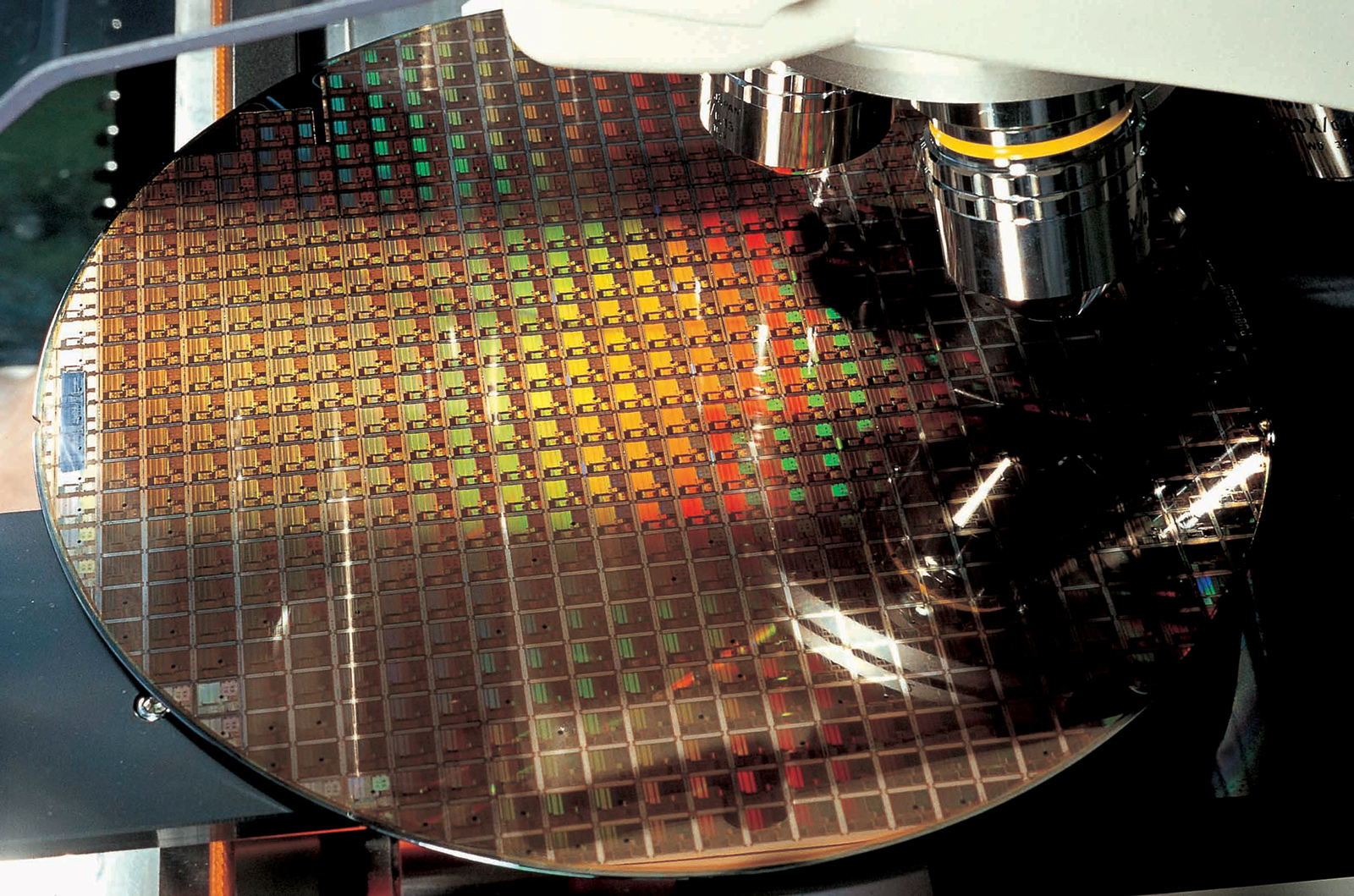
According to a publication by TSMC, NTU, and MIT in Nature (noticed by Verdict), Taiwan Semiconductor Manufacturing Co. (TSMC) and its research partners from the National University of Taiwan (NTU) and Massachusetts Institute of Technology (MIT) have said that they have developed material that will be used for transistor contact electrodes with an upcoming 1nm fabrication process.
Every new process technology brings new challenges and in this case the key challenges are finding the right transistor structure as well as the right transistor materials. Meanwhile, transistor contacts that bring power to transistors are crucial for their performance. Further miniaturization of the semiconductor process technologies increases resistance at contacts, which limits their performance. Therefore, TSMC and other chip makers need to find a contact material that has a very low resistance, can transfer high currents, and can be used for volume production.
The publication indicates that usage of semi-metal bismuth (Bi) as the transistor’s contact electrode can greatly reduce the resistance and increase the current. TSMC currently uses tungsten interconnects (made using selective tungsten deposition process), whereas Intel uses cobalt interconnects. Both have their advantages and both require specific factory tools.
In a bid to use semi-metal bismuth (Bi) as transistor’s contact electrode, researchers had to use a helium ion beam (HIB) lithography system and design an ‘easy deposition process.’ This ‘process’ was only used on an R&D production line, so it is not quite ready for mass production.
Right now, TSMC’s 1nm node is in path-finding mode and the foundry is experimenting with various options. TSMC’s 1nm fabrication process will not be used for high volume manufacturing for years to come and it is not guaranteed that semi-metal bismuth will indeed be used at all. Nonetheless, it is evident that TSMC is already working on its 1nm technology.
