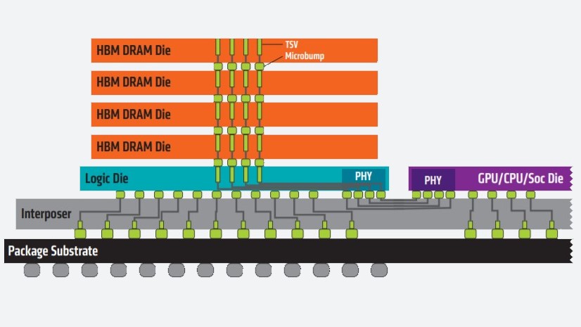
HBM stands for high bandwidth memory and is a type of memory interface used in 3D-stacked DRAM (dynamic random access memory) in some AMD GPUs (aka graphics cards), as well as the server, high-performance computing (HPC) and networking and client space. Samsung and SK Hynix make HBM chips.
Ultimately, HBM is meant to offer much higher bandwidth, lower power consumption compared to the GDDR memory used in most of today’s best graphics cards for gaming.
HBM Specs
| HBM2 / HBM2E (Current) | HBM | HBM3 (Upcoming) | |
| Max Pin Transfer Rate | 3.2 Gbps | 1 Gbps | ? |
| Max Capacity | 24GB | 4GB | 64GB |
| Max Bandwidth | 410 GBps | 128 GBps | 512 GBps |
HBM technology works by vertically stacking memory chips on top of one another in order to shorten how far data has to travel, while allowing for smaller form factors. Additionally, with two 128-bit channels per die, HBM’s memory bus is much wider than that of other types of DRAM memory.
Stacked memory chips are connected through through-silicon vias (TSVs) and microbumps and connect to GPU via the interposer, rather than on-chip.
HBM2 and HBM2E
HBM2 debuted in 2016, and in December 2018, the JEDEC updated the HBM2 standard. The updated standard was commonly referred to as both HBM2 and HBM2E (to denote the deviation from the original HBM2 standard). However, the spec was updated again in early 2020, and the name “HBM2E” wasn’t formally included. However, you may still see people and/or companies refer to HBM2 as HBM2E or even HBMnext, thanks to Micron.
The current HBM2 standard allows for a bandwidth of 3.2 GBps per pin with a max capacity of 24GB per stack (2GB per die across 12 dies per stack) and max bandwidth of 410 GBps, delivered across a 1,024-bit memory interface separated by 8 unique channels on each stack.
Originally, HBM2 was specced for a max transfer rate of 2 GBps per pin, a max capacity of 8GB per stack (1GB max die capacity across 8 dies per stack) and max bandwidth of 256 GBps. It was then bumped to 2.4 Gbps per pin and a max capacity of 24GB (2GB per die across 12 dies per stack) and a 307 Gbps max bandwidth before reaching the standard we see today.
HBM3
While not yet available, the HBM3 standard is currently in discussion and being standardized by JEDEC.
According to an Ars Technica report, HBM3 is expected to support up to 64GB capacities and a bandwidth of up to 512 GBps. In 2019, Jeongdong Choe, an analyst at TechInsights, pointed to HBM3 supporting 4 Gbps transfer rates in an interview with Semiconductor Engineering. HBM3 will also reportedly deliver more dies per stack and more than two times the density per die with a similar power budget. In a 2020 blog post, Cadence reported that the spec will use a 512-bit bus with higher clocks, allowing HBM3 to “achieve the same higher bandwidth with much lower cost by not requiring a silicon interposer.”
We don’t know the release date of HBM3 yet; however, this April we saw SiFive tape out a system-on-chip (SoC) with HBM3.
This article is part of the Tom’s Hardware Glossary.
Further reading:
- Best Graphics Cards
- GPU Benchmarks and Hierarchy
