Our Verdict
Intel’s SSD 670p delivers on both speed and security with faster throughput and hardware encryption support. While Intel’s SSD 670p leverages QLC flash, it is tweaked and tuned where it matters, making it a stellar consumer-oriented PCIe 3.0 NVMe SSD.
For
- Solid performance
- Large dynamic SLC cache with fast recovery
- AES 256-bit hardware encryption
- Software package
- 5-year warranty
Against
- High launch MSRP
- Slow write speeds after the SLC cache fills
- Low endurance compared to TLC SSDs
Features and Specifications
Intel’s SSD 670p rocks an updated PCIe 3.0 x4 controller and the company’s new 144-Layer QLC flash, offering up efficient and performant storage in a slim-yet-spacious M.2 package. It also comes with AES 256-bit hardware encryption support, making it a secure pick for those with sensitive data.
Intel’s SSD 6-series M.2 NVMe SSDs brought Intel’s QLC flash to the mainstream market. With bargain price points and plenty of capacity, both the SSD 660p and SSD 665p have been excellent options for value seekers willing to accept less-than-mainstream levels of performance. However, while responsive, these SSDs couldn’t quite keep pace with the best SSDs on the market and lacked the endurance ratings we have grown accustomed to with TLC flash-based SSDs.
While those SSDs have historically been good budget picks, Intel’s SSD 670p aims to take the SSD 6 series to another level. Intel’s SSD 670p is more than a simple revision — the low-cost M.2 SSD comes with the latest leading-edge NAND technology, improved endurance, and plenty of optimizations for office productivity and gaming.
Specifications
| SSD 670p 512GB | SSD 670p 1TB | SSD 670p 2TB | |
|---|---|---|---|
| Pricing | $89.00 | $154.00 | $329.00 |
| Capacity (User / Raw) | 512GB / 512GB | 1024GB / 1024GB | 2048GB / 2048GB |
| Form Factor | M.2 2280 | M.2 2280 | M.2 2280 |
| Interface / Protocol | PCIe 3.0 x4 / NVMe 1.3 | PCIe 3.0 x4 / NVMe 1.3 | PCIe 3.0 x4 / NVMe 1.3 |
| Controller | Silicon Motion SM2265 | Silicon Motion SM2265 | Silicon Motion SM2265 |
| DRAM | DDR3L | DDR3L | DDR3L |
| Memory | Intel 144L QLC | Intel 144L QLC | Intel 144L QLC |
| Sequential Read | 3,000 MBps | 3,500 MBps | 3,500 MBps |
| Sequential Write | 1,600 MBps | 2,500 MBps | 2,700 MBps |
| Random Read (QD1) | 20,000 IOPS | 20,000 IOPS | 20,000 IOPS |
| Random Write (QD1) | 54,000 IOPS | 54,000 IOPS | 54,000 IOPS |
| Random Read | 110,000 IOPS | 220,000 IOPS | 310,000 IOPS |
| Random Write | 315,000 IOPS | 330,000 IOPS | 340,000 IOPS |
| Security | AES 256-bit FDE | AES 256-bit FDE | AES 256-bit FDE |
| Endurance (TBW) | 185 TB | 370 TB | 740 TB |
| Part Number | SSDPEKNU512GZX1 | SSDPEKNU010TZX1 | SSDPEKNU020TZX1 |
| Warranty | 5-Years | 5-Years | 5-Years |
The SSD 670p is available in capacities of up to 2TB with pricing that ranges from $0.15-$0.17 per gigabyte. Intel tweaked and tuned the drives for low queue depth requests, making them snappy in everyday desktop PC tasks, and also focused on tuning for mixed read/write workloads to assure strong performance in more demanding workloads.
The SSD 670p can deliver up to 3.5/2.7 GBps of sequential read/write throughput and sustain up to 20,000/54,000 random read/write IOPS at a queue depth (QD) of 1, an important metric to quantify snappiness during non-demanding tasks. Peak performance reaches up to 310,000/340,000 random read/write IOPS at a queue depth of 256. Notably, these specifications are based on the SSD’s dynamic SLC cache. Because cache performance is so important, Intel optimized the design to improve performance when the drive is nearly full.
Like the SSD 665p, the 2TB SSD 670p’s cache measures up to 280GB when the device is empty, but the dynamic cache remains available until the drive is 85% full, an improvement over the 75% threshold with the older drive. At that point and beyond, the drive will operate with only a static SLC cache that measures 6GB per 512GB of capacity.
Intel’s SSD 670p features global wear-leveling and supports robust LDPC error correction capabilities, end-to-end data path protection, and DRAM ECC and SRAM ECC for data reliability. These, in conjunction with the new flash’s enhancements, enable Intel to back the Intel SSD 670p with a five-year warranty and improve its write endurance over its predecessor. The 670p’s write endurance rating is 185 TBW for every 512GB of capacity, but the drive is only overprovisioned by 7% from the factory (2% less than Samsung drives, on average).
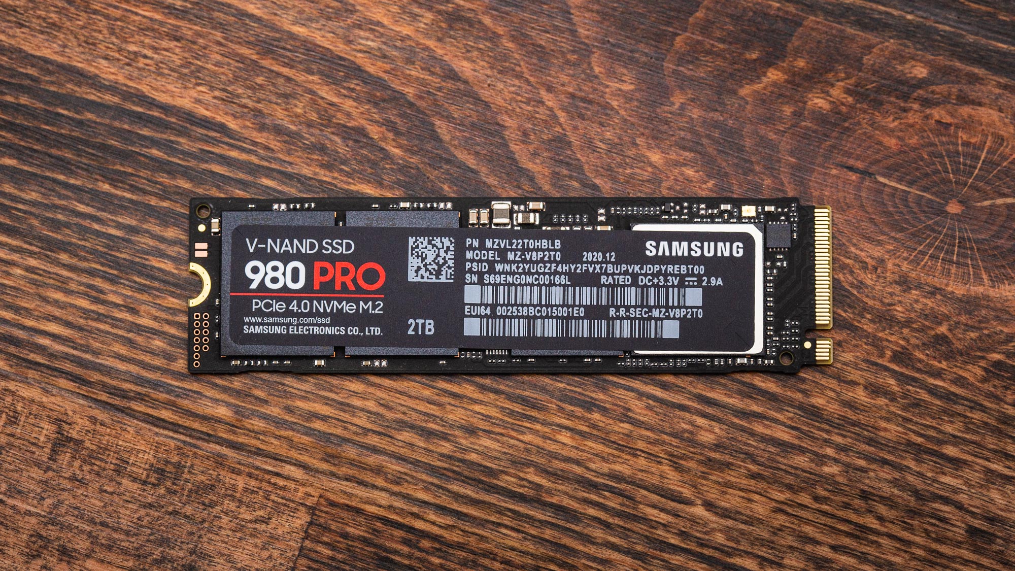
While Intel has improved the SSD 670p’s endurance rating over its predecessors (endurance jumps from 100-150TBW per 512GB to 185TBW), the drive still can’t entirely overcome the endurance penalties associated with QLC flash. For instance, the Adata XPG Gammix S50 Lite comes with TLC flash and features 370TBW per 512GB of capacity, while the TLC-powered Samsung 970 Evo Plus comes with 300TBW per 512GB of capacity. The SSD 670p trails these drives in endurance but most consumers will write roughly 60-160TB of data in five years, meaning the 670p should provide plenty of endurance for a typical user.
Software and Accessories
Image 1 of 3
Image 2 of 3
Image 3 of 3
Intel supports the SSD 670p with the Intel Memory and Storage Tool (Intel MAS). This software allows you to monitor drive health, run diagnostic tests, update the firmware, and manually clear the SLC cache. Additionally, Intel provides an NVMe driver for its consumer SSDs, but at the time of publication, the latest downloadable version (version 5.1.0.1003) will not install on the SSD 670p.
A Closer Look
Image 1 of 3
Image 2 of 3
Image 3 of 3
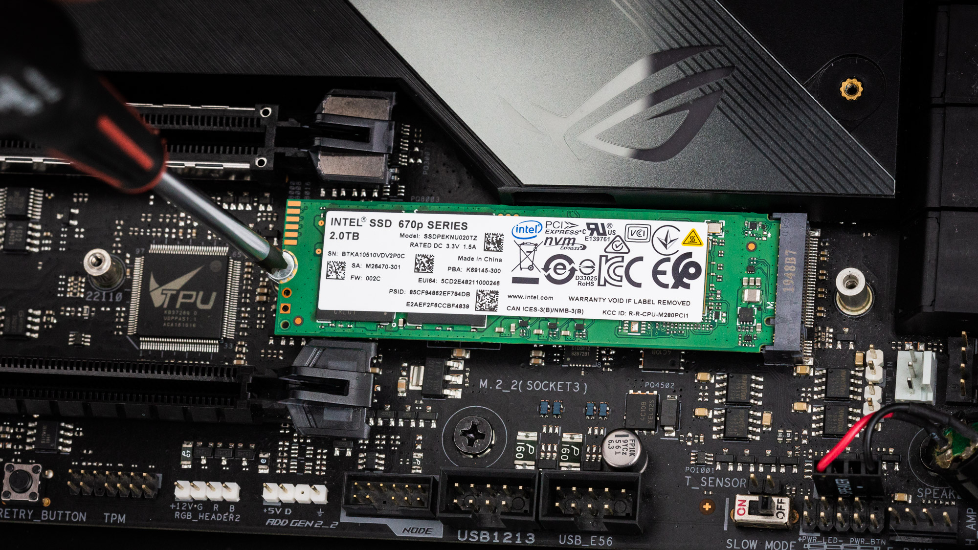
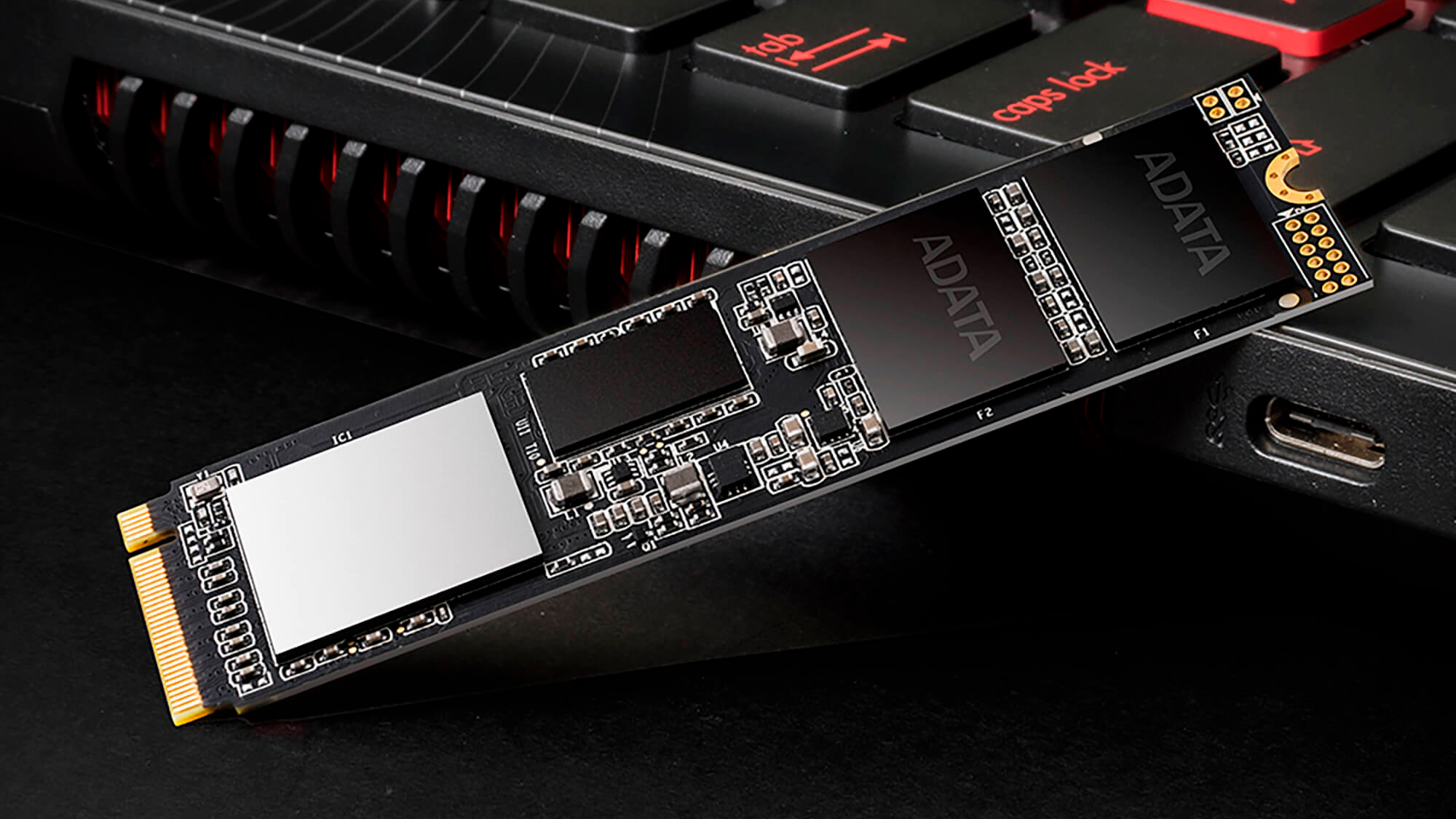
Intel’s SSD 670p comes in an M.2 2280 single-sided form factor for compatibility with the latest thin and light devices. Aesthetically, the SSD 670p’s green PCB and the white sticker aren’t the most attractive, but that only matters if you’re going to place the drive inside a new desktop build with a see-through panel and leave it exposed without a heatsink.
Image 1 of 2
Image 2 of 2
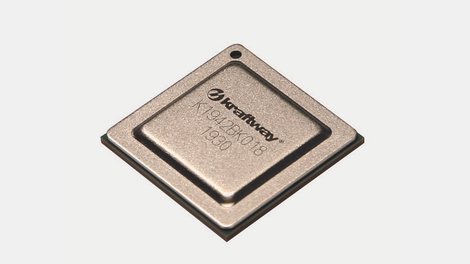
The SSD 670p uses a custom Silicon Motion’s SM2265 controller, one of the company’s latest NVMe SSDs controllers specifically optimized for use with Intel’s latest 144-Layer 3D QLC flash. The SM2265’s architecture is similar to the SM2267 that powers the Adata XPG Gammix S50 Lite, but it lacks the higher-bandwidth PCIe Gen4 interface, employing a Gen3 PHY instead.
The SM2265 leverages two Arm Cortex R5 CPU cores for I/O processing and interfaces with a single 2Gb Nanya DDR3L-1866 DRAM chip to buffer FTL metadata. It’s produced on a 28nm process node for cost-effective production and cool thermals. The drive also supports power-saving features, including ASPM, APST, and L1.2 sleep (rated at just 3mW of consumption), along with hardware-accelerated AES 256-bit encryption with support for Pyrite 2.0 for the security-conscious.
Our 2TB sample comes armed with sixteen dies of Intel’s latest 144-Layer QLC flash, with eight dies per package. These dies interface with the controller at frequencies up to 1,200 MTps over four flash channels, up from 667 MTps with Intel’s previous-gen flash. Part of that improvement stems from scaling to the highest bit densities (13.8 Gb/mm^2) and layer heights the company has ever achieved. To reach 144 layers, Intel has moved to a 3-deck stack (48+48+48 layers) design, an industry first for mass-produced flash.
In this block-by-deck architecture, Intel separates each deck with a dummy layer, and each deck can operate as either SLC or QLC. For more efficient block erases, each deck can be erased without touching the data stored on the other decks. Intel says this approach helps tremendously with garbage collection and boosts quality of service (QoS) significantly.
The flash architecture also incorporates CMOS under the array (CuA) tech to boost density and features quad-plane access to enhance parallelism. Intel uses a floating gate cell design to optimize die space and boost data retention. Intel also claims the design can handle more parallel data operations.
Image 1 of 3
Image 2 of 3
Image 3 of 3
Intel also implemented a new independent multi-plane read operation (IMPRO) technique to double the number of read operations by splitting the four planes into dual two-plane groups that can be read asynchronously, allowing the SSD to simultaneously read from the TLC and QLC portions of the flash. The asynchronous nature of IMPRO can create noise coupling. To mitigate that effect, Intel configures the charge-pumps, wordline/bitline regulators, and drop-out (LDO) regulators to drive separate loads in each plane group.
Additionally, to address the sensitivity of QLC technology and reduce first-pass program penalties, the flash features a 4-16 multi-pass programming algorithm and a 1-2-6-6 Gray code. The cells are optimized via a quad-level dynamic start technique that first programs the cell to a 4-level state, and then after the data is read from the cells, the cells are programmed into the final 16-state level.
MORE: Best SSDs
MORE: How We Test HDDs And SSDs
MORE: All SSD Content
Current page:
Features and Specifications
Next Page 2TB Performance Results
