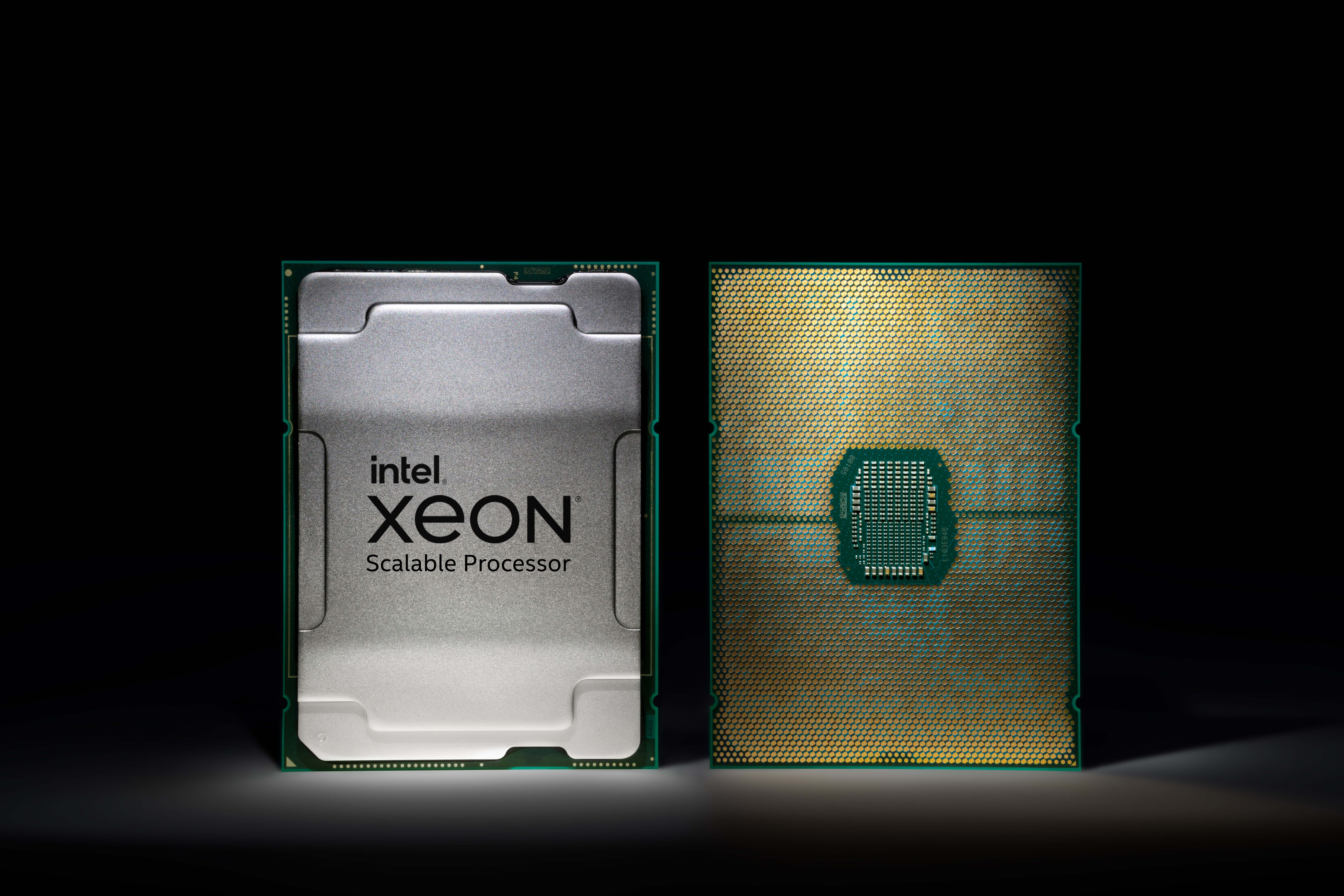
Intel’s long-delayed 10nm+ third-gen Xeon Scalable Ice Lake processors mark an important step forward for the company as it attempts to fend off intense competition from AMD’s 7nm EPYC Milan processors that top out at 64 cores, a key advantage over Intel’s existing 14nm Cascade Lake Refresh that tops out at 28 cores. The 40-core Xeon Platinum 8380 serves as the flagship model of Intel’s revamped lineup, which the company says features up to a 20% IPC uplift on the strength of the new Sunny Cove core architecture paired with the 10nm+ process.
Intel has already shipped over 200,000 units to its largest customers since the beginning of the year, but today marks the official public debut of its newest lineup of data center processors, so we get to share benchmarks. The Ice Lake chips drop into dual-socket Whitley server platforms, while the previously-announced Cooper Lake slots in for quad- and octo-socket servers. Intel has slashed Xeon pricing up to 60% to remain competitive with EPYC Rome, and with EPYC Milan now shipping, the company has reduced per-core pricing again with Ice Lake to remain competitive as it targets high-growth markets, like the cloud, enterprise, HPC, 5G, and the edge.
The new Xeon Scalable lineup comes with plenty of improvements, like increased support for up to eight memory channels that run at a peak of DDR4-3200 with two DIMMs per channel, a notable improvement over Cascade Lake’s support for six channels at DDR4-2933 and matching EPYC’s eight channels of memory. Ice Lake also supports 6TB of DRAM/Optane per socket (4TB of DRAM) and 4TB of Optane Persistent Memory DIMMs per socket (8 TB in dual-socket). Unlike Intel’s past practices, Ice Lake also supports the full memory and Optane capacity on all models with no additional upcharge.
Intel has also moved forward from 48 lanes of PCIe 3.0 connectivity to 64 lanes of PCIe 4.0 (128 lanes in dual-socket), improving both I/O bandwidth and increasing connectivity to match AMD’s 128 available lanes in a dual-socket server.
Intel says that these additives, coupled with a range of new SoC-level optimizations, a focus on improved power management, along with support for new instructions, yield an average of 46% more performance in a wide range of data center workloads. Intel also claims a 50% uplift to latency-sensitive applications, like HammerDB, Java, MySQL, and WordPress, and up to 57% more performance in heavily-threaded workloads, like NAMD, signaling that the company could return to a competitive footing in what has become one of AMD’s strongholds — heavily threaded workloads. We’ll put that to the test shortly. First, let’s take a closer look at the lineup.
Intel Third-Gen Xeon Scalable Ice Lake Pricing and Specfications
We have quite the list of chips below, but we’ve actually filtered out the downstream Intel parts, focusing instead on the high-end ‘per-core scalable’ models. All told, the Ice Lake family spans 42 SKUs, with many of the lower-TDP (and thus performance) models falling into the ‘scalable performance’ category.
Intel also has specialized SKUs targeted at maximum SGX enclave capacity, cloud-optimized for VMs, liquid-cooled, networking/NFV, media, long-life and thermal-friendly, and single-socket optimized parts, all of which you can find in the slide a bit further below.
| Cores / Threads | Base / Boost – All Core (GHz) | L3 Cache (MB) | TDP (W) | 1K Unit Price / RCP | |
| EPYC Milan 7763 | 64 / 128 | 2.45 / 3.5 | 256 | 280 | $7,890 |
| EPYC Rome 7742 | 64 / 128 | 2.25 / 3.4 | 256 | 225 | $6,950 |
| EPYC Milan 7663 | 56 / 112 | 2.0 / 3.5 | 256 | 240 | $6,366 |
| EPYC Milan 7643 | 48 / 96 | 2.3 / 3.6 | 256 | 225 | $4.995 |
| Xeon Platinum 8380 | 40 / 80 | 2.3 / 3.2 – 3.0 | 60 | 270 | $8,099 |
| Xeon Platinum 8368 | 38 / 76 | 2.4 / 3.4 – 3.2 | 57 | 270 | $6,302 |
| Xeon Platinum 8360Y | 36 / 72 | 2.4 / 3.5 – 3.1 | 54 | 250 | $4,702 |
| Xeon Platinum 8362 | 32 / 64 | 2.8 / 3.6 – 3.5 | 48 | 265 | $5,448 |
| EPYC Milan 7F53 | 32 / 64 | 2.95 / 4.0 | 256 | 280 | $4,860 |
| EPYC Milan 7453 | 28 / 56 | 2.75 / 3.45 | 64 | 225 | $1,570 |
| Xeon Gold 6348 | 28 / 56 | 2.6 / 3.5 – 3.4 | 42 | 235 | $3,072 |
| Xeon Platinum 8280 | 28 / 56 | 2.7 / 4.0 – 3.3 | 38.5 | 205 | $10,009 |
| Xeon Gold 6258R | 28 / 56 | 2.7 / 4.0 – 3.3 | 38.5 | 205 | $3,651 |
| EPYC Milan 74F3 | 24 / 48 | 3.2 / 4.0 | 256 | 240 | $2,900 |
| Intel Xeon Gold 6342 | 24 / 48 | 2.8 / 3.5 – 3.3 | 36 | 230 | $2,529 |
| Xeon Gold 6248R | 24 / 48 | 3.0 / 4.0 | 35.75 | 205 | $2,700 |
| EPYC Milan 7443 | 24 / 48 | 2.85 / 4.0 | 128 | 200 | $2,010 |
| Xeon Gold 6354 | 18 / 36 | 3.0 / 3.6 – 3.6 | 39 | 205 | $2,445 |
| EPYC Milan 73F3 | 16 / 32 | 3.5 / 4.0 | 256 | 240 | $3,521 |
| Xeon Gold 6346 | 16 / 32 | 3.1 / 3.6 – 3.6 | 36 | 205 | $2,300 |
| Xeon Gold 6246R | 16 / 32 | 3.4 / 4.1 | 35.75 | 205 | $3,286 |
| EPYC Milan 7343 | 16 / 32 | 3.2 / 3.9 | 128 | 190 | $1,565 |
| Xeon Gold 5317 | 12 / 24 | 3.0 / 3.6 – 3.4 | 18 | 150 | $950 |
| Xeon Gold 6334 | 8 / 16 | 3.6 / 3.7 – 3.6 | 18 | 165 | $2,214 |
| EPYC Milan 72F3 | 8 / 16 | 3.7 / 4.1 | 256 | 180 | $2,468 |
| Xeon Gold 6250 | 8 / 16 | 3.9 / 4.5 | 35.75 | 185 | $3,400 |
At 40 cores, the Xeon Platinum 8380 reaches new heights over its predecessors that topped out at 28 cores, striking higher in AMD’s Milan stack. The 8380 comes at $202 per core, which is well above the $130-per-core price tag on the previous-gen flagship, the 28-core Xeon 6258R. However, it’s far less expensive than the $357-per-core pricing of the Xeon 8280, which had a $10,008 price tag before AMD’s EPYC upset Intel’s pricing model and forced drastic price reductions.
With peak clock speeds of 3.2 GHz, the 8380 has a much lower peak clock rate than the previous-gen 28-core 6258R’s 4.0 GHz. Even dipping down to the new 28-core Ice Lake 6348 only finds peak clock speeds of 3.5 GHz, which still trails the Cascade Lake-era models. Intel obviously hopes to offset those reduced clock speeds with other refinements, like increased IPC and better power and thermal management.
On that note, Ice Lake tops out at 3.7 GHz on a single core, and you’ll have to step down to the eight-core model to access these clock rates. In contrast, Intel’s previous-gen eight-core 6250 had the highest clock rate, 4.5 GHz, of the Cascade Lake stack.
Surprisingly, AMD’s EPYC Milan models actually have higher peak frequencies than the Ice Lake chips at any given core count, but remember, AMD’s frequencies are only guaranteed on one physical core. In contrast, Intel specs its chips to deliver peak clock rates on any core. Both approaches have their merits, but AMD’s more refined boost tech paired with the 7nm TSMC process could pay dividends for lightly-threaded work. Conversely, Intel does have solid all-core clock rates that peak at 3.6 GHz, whereas AMD has more of a sliding scale that varies based on the workload, making it hard to suss out the winners by just examining the spec sheet.
Ice Lake’s TDPs stretch from 85W up to 270W. Surprisingly, despite the lowered base and boost clocks, Ice Lake’s TDPs have increased gen-on-gen for the 18-, 24- and 28-core models. Intel is obviously pushing higher on the TDP envelope to extract the most performance out of the socket possible, but it does have lower-power chip options available (listed in the graphic below).
AMD has a notable hole in its Milan stack at both the 12- and 18-core mark, a gap that Intel has filled with its Gold 5317 and 6354, respectively. Milan still holds the top of the hierarchy with 48-, 56- and 64-core models.
Image 1 of 12
Image 2 of 12
Image 3 of 12
Image 4 of 12
Image 5 of 12
Image 6 of 12
Image 7 of 12
Image 8 of 12
Image 9 of 12
Image 10 of 12
Image 11 of 12
Image 12 of 12
The Ice Lake Xeon chips drop into Whitley server platforms with Socket LGA4189-4/5. The FC-LGA14 package measures 77.5mm x 56.5mm and has an LGA interface with 4189 pins. The die itself is predicted to measure ~600mm2, though Intel no longer shares details about die sizes or transistor counts. In dual-socket servers, the chips communicate with each other via three UPI links that operate at 11.2 GT/s, an increase from 10.4 GT/s with Cascade Lake. . The processor interfaces with the C620A chipset via four DMI 3.0 links, meaning it communicates at roughly PCIe 3.0 speeds.
The C620A chipset also doesn’t support PCIe 4.0; instead, it supports up to 20 lanes of PCIe 3.0, ten USB 3.0, and fourteen USB 2.0 ports, along with 14 ports of SATA 6 Gbps connectivity. Naturally, that’s offset by the 64 PCIe 4.0 lanes that come directly from the processor. As before, Intel offers versions of the chipset with its QuickAssist Technology (QAT), which boosts performance in cryptography and compression/decompression workloads.
Image 1 of 12
Image 2 of 12
Image 3 of 12
Image 4 of 12
Image 5 of 12
Image 6 of 12
Image 7 of 12
Image 8 of 12
Image 9 of 12
Image 10 of 12
Image 11 of 12
Image 12 of 12
Intel’s focus on its platform adjacencies business is a key part of its messaging around the Ice Lake launch — the company wants to drive home its message that coupling its processors with its own differentiated platform additives can expose additional benefits for Whitley server platforms.
The company introduced new PCIe 4.0 solutions, including the new 200 GbE Ethernet 800 Series adaptors that sport a PCIe 4.0 x16 connection and support RDMA iWARP and RoCEv2, and the Intel Optane SSD P5800X, a PCIe 4.0 SSD that uses ultra-fast 3D XPoint media to deliver stunning performance results compared to typical NAND-based storage solutions.
Intel also touts its PCIe 4.0 SSD D5-P5316, which uses the company’s 144-Layer QLC NAND for read-intensive workloads. These SSDs offer up to 7GBps of throughput and come in capacities stretching up to 15.36 TB in the U.2 form factor, and 30.72 TB in the E1.L ‘Ruler’ form factor.
Intel’s Optane Persistent Memory 200-series offers memory-addressable persistent memory in a DIMM form factor. This tech can radically boost memory capacity up to 4TB per socket in exchange for higher latencies that can be offset through software optimizations, thus yielding more performance in workloads that are sensitive to memory capacity.
The “Barlow Pass” Optane Persistent Memory 200 series DIMMs promise 30% more memory bandwidth than the previous-gen Apache Pass models. Capacity remains at a maximum of 512GB per DIMM with 128GB and 256GB available, and memory speeds remain at a maximum of DDR4-2666.
Intel has also expanded its portfolio of Market Ready and Select Solutions offerings, which are pre-configured servers for various workloads that are available in over 500 designs from Intel’s partners. These simple-to-deploy servers are designed for edge, network, and enterprise environments, but Intel has also seen uptake with cloud service providers like AWS, which uses these solutions for its ParallelCluster HPC service.
Image 1 of 10
Image 2 of 10
Image 3 of 10
Image 4 of 10
Image 5 of 10
Image 6 of 10
Image 7 of 10
Image 8 of 10
Image 9 of 10
Image 10 of 10
Like the benchmarks you’ll see in this review, the majority of performance measurements focus on raw throughput. However, in real-world environments, a combination of throughput and responsiveness is key to deliver on latency-sensitive SLAs, particularly in multi-tenant cloud environments. Factors such as loaded latency (i.e., the amount of performance delivered to any number of applications when all cores have varying load levels) are key to ensuring performance consistency across multiple users. Ensuring consistency is especially challenging with diverse workloads running on separate cores in multi-tenant environments.
Intel says it focused on performance consistency in these types of environments through a host of compute, I/O, and memory optimizations. The cores, naturally, benefit from increased IPC, new ISA instructions, and scaling up to higher core counts via the density advantages of 10nm, but Intel also beefed up its I/O subsystem to 64 lanes of PCIe 4.0, which improves both connectivity (up from 48 lanes) and throughput (up from PCIe 3.0).
Intel says it designed the caches, memory, and I/O, not to mention power levels, to deliver consistent performance during high utilization. As seen in slide 30, the company claims these alterations result in improved application performance and latency consistency by reducing long tail latencies to improve worst-case performance metrics, particularly for memory-bound and multi-tenant workloads.
Image 1 of 12
Image 2 of 12
Image 3 of 12
Image 4 of 12
Image 5 of 12
Image 6 of 12
Image 7 of 12
Image 8 of 12
Image 9 of 12
Image 10 of 12
Image 11 of 12
Image 12 of 12
Ice Lake brings a big realignment of the company’s die that provides cache, memory, and throughput advances. The coherent mesh interconnect returns with a similar arrangement of horizontal and vertical rings present on the Cascade Lake-SP lineup, but with a realignment of the various elements, like cores, UPI connections, and the eight DDR4 memory channels that are now split into four dual-channel controllers. Here we can see that Intel shuffled around the cores on the 28-core die and now has two execution cores on the bottom of the die clustered with I/O controllers (some I/O is now also at the bottom of the die).
Intel redesigned the chip to support two new sideband fabrics, one controlling power management and the other used for general-purpose management traffic. These provide telemetry data and control to the various IP blocks, like execution cores, memory controllers, and PCIe/UPI controllers.
The die includes a separate peer-to-peer (P2P) fabric to improve bandwidth between cores, and the I/O subsystem was also virtualized, which Intel says offers up to three times the fabric bandwidth compared to Cascade Lake. Intel also split one of the UPI blocks into two, creating a total of three UPI links, all with fine-grained power control of the UPI links. Now, courtesy of dedicated PLLs, all three UPIs can modulate clock frequencies independently based on load.
Densely packed AVX instructions augment performance in properly-tuned workloads at the expense of higher power consumption and thermal load. Intel’s Cascade Lake CPUs drop to lower frequencies (~600 to 900 MHz) during AVX-, AVX2-, and AVX-512-optimized workloads, which has hindered broader adoption of AVX code.
To reduce the impact, Intel has recharacterized its AVX power limits, thus yielding (unspecified) higher frequencies for AVX-512 and AVX-256 operations. This is done in an adaptive manner based on three different power levels for varying instruction types. This nearly eliminates the frequency delta between AVX and SSE for 256-heavy and 512-light operations, while 512-heavy operations have also seen significant uplift. All Ice Lake SKUs come with dual 512b FMAs, so this optimization will pay off across the entire stack.
Intel also added support for a host of new instructions to boost cryptography performance, like VPMADD52, GFNI, SHA-NI, Vector AES, and Vector Carry-Less multiply instructions, and a few new instructions to boost compression/decompression performance. All rely heavily upon AVX acceleration. The chips also support Intel’s Total Memory Encryption (TME) that offers DRAM encryption through AES-XTS 128-bit hardware-generated keys.
Intel also made plenty of impressive steps forward on the microarchitecture, with improvements to every level of the pipeline allowing Ice Lake’s 10nm Sunny Cove cores to deliver far higher IPC than 14nm Cascade Lake’s Skylake-derivative architecture. Key improvements to the front end include larger reorder, load, and store buffers, along with larger reservation stations. Intel increased the L1 data cache from 32 KiB, the capacity it has used in its chips for a decade, to 42 KiB, and moved from 8-way to 12-way associativity. The L2 cache moves from 4-way to 8-way and is also larger, but the capacity is dependent upon each specific type of product — for Ice Lake server chips, it weighs in at 1.25 MB per core.
Intel expanded the micro-op cache (UOP) from 1.5K to 2.25K micro-ops, the second-level translation lookaside buffer (TLB) from 1536 entries to 2048, and moved from a four-wide allocation to five-wide to allow the in-order portion of the pipeline (front end) to feed the out-of-order (back end) portion faster. Additionally, Intel expanded the Out of Order (OoO) Window from 224 to 352. Intel also increased the number of execution units to handle ten operations per cycle (up from eight with Skylake) and focused on improving branch prediction accuracy and reducing latency under load conditions.
The store unit can now process two store data operations for every cycle (up from one), and the address generation units (AGU) also handle two loads and two stores each cycle. These improvements are necessary to match the increased bandwidth from the larger L1 data cache, which does two reads and two writes every cycle. Intel also tweaked the design of the sub-blocks in the execution units to enable data shuffles within the registers.
Intel also added support for its Software Guard Extensions (SGX) feature that debuted with the Xeon E lineup, and increased capacity to 1TB (maximum capacity varies by model). SGX creates secure enclaves in an encrypted portion of the memory that is exclusive to the code running in the enclave – no other process can access this area of memory.
Test Setup
We have a glaring hole in our test pool: Unfortunately, we do not have AMD’s recently-launched EPYC Milan processors available for this round of benchmarking, though we are working on securing samples and will add competitive benchmarks when available.
We do have test results for the AMD’s frequency-optimized Rome 7Fx2 processors, which represent AMD’s performance with its previous-gen chips. As such, we should view this round of tests largely through the prism of Intel’s gen-on-gen Xeon performance improvement, and not as a measure of the current state of play in the server chip market.
We use the Xeon Platinum Gold 8280 as a stand-in for the less expensive Xeon Gold 6258R. These two chips are identical and provide the same level of performance, with the difference boiling down to the more expensive 8280 coming with support for quad-socket servers, while the Xeon Gold 6258R tops out at dual-socket support.
Image 1 of 7
Image 2 of 7
Image 3 of 7
Image 4 of 7
Image 5 of 7
Image 6 of 7
Image 7 of 7
Intel provided us with a 2U Server System S2W3SIL4Q Software Development Platform with the Coyote Pass server board for our testing. This system is designed primarily for validation purposes, so it doesn’t have too many noteworthy features. The system is heavily optimized for airflow, with the eight 2.5″ storage bays flanked by large empty bays that allow for plenty of air intake.
The system comes armed with dual redundant 2100W power supplies, a 7.68TB Intel SSD P5510, an 800GB Optane SSD P5800X, and an E810-CQDA2 200GbE NIC. We used the Intel SSD P5510 for our benchmarks and cranked up the fans for maximum performance in our benchmarks.
We tested with the pre-installed 16x 32GB DDR4-3200 DIMMs, but Intel also provided sixteen 128GB Optane Persistent Memory DIMMs for further testing. Due to time constraints, we haven’t yet had time to test the Optane DIMMs, but stay tuned for a few demo workloads in a future article. As we’re not entirely done with our testing, we don’t want to risk prying the 8380 out of the socket yet for pictures — the large sockets from both vendors are becoming more finicky after multiple chip reinstalls.
| Memory | Tested Processors | |
|---|---|---|
| Intel S2W3SIL4Q | 16x 32GB SK hynix ECC DDR4-3200 | Intel Xeon Platinum 8380 |
| Supermicro AS-1023US-TR4 | 16x 32GB Samsung ECC DDR4-3200 | EPYC 7742, 7F72, 7F52 |
| Dell/EMC PowerEdge R460 | 12x 32GB SK hynix DDR4-2933 | Intel Xeon 8280, 6258R, 5220R, 6226R |
To assess performance with a range of different potential configurations, we used a Supermicro 1024US-TR4 server with three different EPYC Rome configurations. We outfitted this server with 16x 32GB Samsung ECC DDR4-3200 memory modules, ensuring the chips had all eight memory channels populated.
We used a Dell/EMC PowerEdge R460 server to test the Xeon processors in our test group. We equipped this server with 12x 32GB Sk hynix DDR4-2933 modules, again ensuring that each Xeon chip’s six memory channels were populated.
We used the Phoronix Test Suite for benchmarking. This automated test suite simplifies running complex benchmarks in the Linux environment. The test suite is maintained by Phoronix, and it installs all needed dependencies and the test library includes 450 benchmarks and 100 test suites (and counting). Phoronix also maintains openbenchmarking.org, which is an online repository for uploading test results into a centralized database.
We used Ubuntu 20.04 LTS to maintain compatibility with our existing test results, and leverage the default Phoronix test configurations with the GCC compiler for all tests below. We also tested all platforms with all available security mitigations.
Naturally, newer Linux kernels, software, and targeted optimizations can yield improvements for any of the tested processors, so take these results as generally indicative of performance in compute-intensive workloads, but not as representative of highly-tuned deployments.
Linux Kernel, GCC and LLVM Compilation Benchmarks
Image 1 of 2
Image 2 of 2
AMD’s EPYC Rome processors took the lead over the Cascade Lake Xeon chips at any given core count in these benchmarks, but here we can see that the 40-core Ice Lake Xeon 8380 has tremendous potential for these type of workloads. The dual 8380 processors complete the Linux compile benchmark, which builds the Linux kernel at default settings, in 20 seconds, edging out the 64-core EPYC Rome 7742 by one second. Naturally, we expect AMD’s Milan flagship, the 7763, to take the lead in this benchmark. Still, the implication is clear — Ice Lake-SP has significantly-improved performance, thus reducing the delta between Xeon and competing chips.
We can also see a marked improvement in the LLVM compile, with the 8380 reducing the time to completion by ~20% over the prior-gen 8280.
Molecular Dynamics and Parallel Compute Benchmarks
Image 1 of 6
Image 2 of 6
Image 3 of 6
Image 4 of 6
Image 5 of 6
Image 6 of 6
NAMD is a parallel molecular dynamics code designed to scale well with additional compute resources; it scales up to 500,000 cores and is one of the premier benchmarks used to quantify performance with simulation code. The Xeon 8380’s notch a 32% improvement in this benchmark, slightly beating the Rome chips.
Stockfish is a chess engine designed for the utmost in scalability across increased core counts — it can scale up to 512 threads. Here we can see that this massively parallel code scales well with EPYC’s leading core counts. The EPYC Rome 7742 retains its leading position at the top of the chart, but the 8380 offers more than twice the performance of the previous-gen Cascade Lake flagship.
We see similarly impressive performance uplifts in other molecular dynamics workloads, like the Gromacs water benchmark that simulates Newtonian equations of motion with hundreds of millions of particles. Here Intel’s dual 8380’s take the lead over the EPYC Rome 7742 while pushing out nearly twice the performance of the 28-core 8280.
We see a similarly impressive generational improvement in the LAAMPS molecular dynamics workload, too. Again, AMD’s Milan will likely be faster than the 7742 in this workload, so it isn’t a given that the 8380 has taken the definitive lead over AMD’s current-gen chips, though it has tremendously improved Intel’s competitive positioning.
The NAS Parallel Benchmarks (NPB) suite characterizes Computational Fluid Dynamics (CFD) applications, and NASA designed it to measure performance from smaller CFD applications up to “embarrassingly parallel” operations. The BT.C test measures Block Tri-Diagonal solver performance, while the LU.C test measures performance with a lower-upper Gauss-Seidel solver. The EPYC Milan 7742 still dominates in this workload, showing that Ice Lake’s broad spate of generational improvements still doesn’t allow Intel to take the lead in all workloads.
Rendering Benchmarks
Image 1 of 4
Image 2 of 4
Image 3 of 4
Image 4 of 4
Turning to more standard fare, provided you can keep the cores fed with data, most modern rendering applications also take full advantage of the compute resources. Given the well-known strengths of EPYC’s core-heavy approach, it isn’t surprising to see the 64-core EPYC 7742 processors retain the lead in the C-Ray benchmark, and that applies to most of the Blender benchmarks, too.
Encoding Benchmarks
Image 1 of 3
Image 2 of 3
Image 3 of 3
Encoders tend to present a different type of challenge: As we can see with the VP9 libvpx benchmark, they often don’t scale well with increased core counts. Instead, they often benefit from per-core performance and other factors, like cache capacity. AMD’s frequency-optimized 7F52 retains its leading position in this benchmark, but Ice Lake again reduces the performance delta.
Newer software encoders, like the Intel-Netflix designed SVT-AV1, are designed to leverage multi-threading more fully to extract faster performance for live encoding/transcoding video applications. EPYC Rome’s increased core counts paired with its strong per-core performance beat Cascade Lake in this benchmark handily, but the step up to forty 10nm+ cores propels Ice Lake to the top of the charts.
Compression, Security and Python Benchmarks
Image 1 of 5
Image 2 of 5
Image 3 of 5
Image 4 of 5
Image 5 of 5
The Pybench and Numpy benchmarks are used as a general litmus test of Python performance, and as we can see, these tests typically don’t scale linearly with increased core counts, instead prizing per-core performance. Despite its somewhat surprisingly low clock rates, the 8380 takes the win in the Pybench benchmark and improves Xeon’s standing in Numpy as it takes a close second to the 7F52.
Compression workloads also come in many flavors. The 7-Zip (p7zip) benchmark exposes the heights of theoretical compression performance because it runs directly from main memory, allowing both memory throughput and core counts to heavily impact performance. As we can see, this benefits the core-heavy chips as they easily dispatch with the chips with lesser core counts. The Xeon 8380 takes the lead in this test, but other independent benchmarks show that AMD’s EPYC Milan would lead this chart.
In contrast, the gzip benchmark, which compresses two copies of the Linux 4.13 kernel source tree, responds well to speedy clock rates, giving the 16-core 7F52 the lead. Here we see that 8380 is slightly slower than the previous-gen 8280, which is likely at least partially attributable to the 8380’s much lower clock rate.
The open-source OpenSSL toolkit uses SSL and TLS protocols to measure RSA 4096-bit performance. As we can see, this test favors the EPYC processors due to its parallelized nature, but the 8380 has again made big strides on the strength of its higher core count. Offloading this type of workload to dedicated accelerators is becoming more common, and Intel also offers its QAT acceleration built into chipsets for environments with heavy requirements.
Conclusion
Admittedly, due to our lack of EPYC Milan samples, our testing today of the Xeon Platinum 8380 is more of a demonstration of Intel’s gen-on-gen performance improvements rather than a holistic view of the current competitive landscape. We’re working to secure a dual-socket Milan server and will update when one lands in our lab.
Overall, Intel’s third-gen Xeon Scalable is a solid step forward for the Xeon franchise. AMD has steadily chewed away data center market share from Intel on the strength of its EPYC processors that have traditionally beaten Intel’s flagships by massive margins in heavily-threaded workloads. As our testing, and testing from other outlets shows, Ice Lake drastically reduces the massive performance deltas between the Xeon and EPYC families, particularly in heavily threaded workloads, placing Intel on a more competitive footing as it faces an unprecedented challenge from AMD.
AMD will still hold the absolute performance crown in some workloads with Milan, but despite EPYC Rome’s commanding lead in the past, progress hasn’t been as swift as some projected. Much of that boils down to the staunchly risk-averse customers in the enterprise and data center; these customers prize a mix of factors beyond the standard measuring stick of performance and price-to-performance ratios, instead focusing on areas like compatibility, security, supply predictability, reliability, serviceability, engineering support, and deeply-integrated OEM-validated platforms.
AMD has improved drastically in these areas and now has a full roster of systems available from OEMs, along with broadening uptake with CSPs and hyperscalers. However, Intel benefits from its incumbency and all the advantages that entails, like wide software optimization capabilities and platform adjacencies like networking, FPGAs, and Optane memory.
Although Ice Lake doesn’t lead in all metrics, it does improve the company’s positioning as it moves forward toward the launch of its Sapphire Rapids processors that are slated to arrive later this year to challenge AMD’s core-heavy models. Intel still holds the advantage in several criteria that appeal to the broader enterprise market, like pre-configured Select Solutions and engineering support. That, coupled with drastic price reductions, has allowed Intel to reduce the impact of a fiercely-competitive adversary. We can expect the company to redouble those efforts as Ice Lake rolls out to the more general server market.
