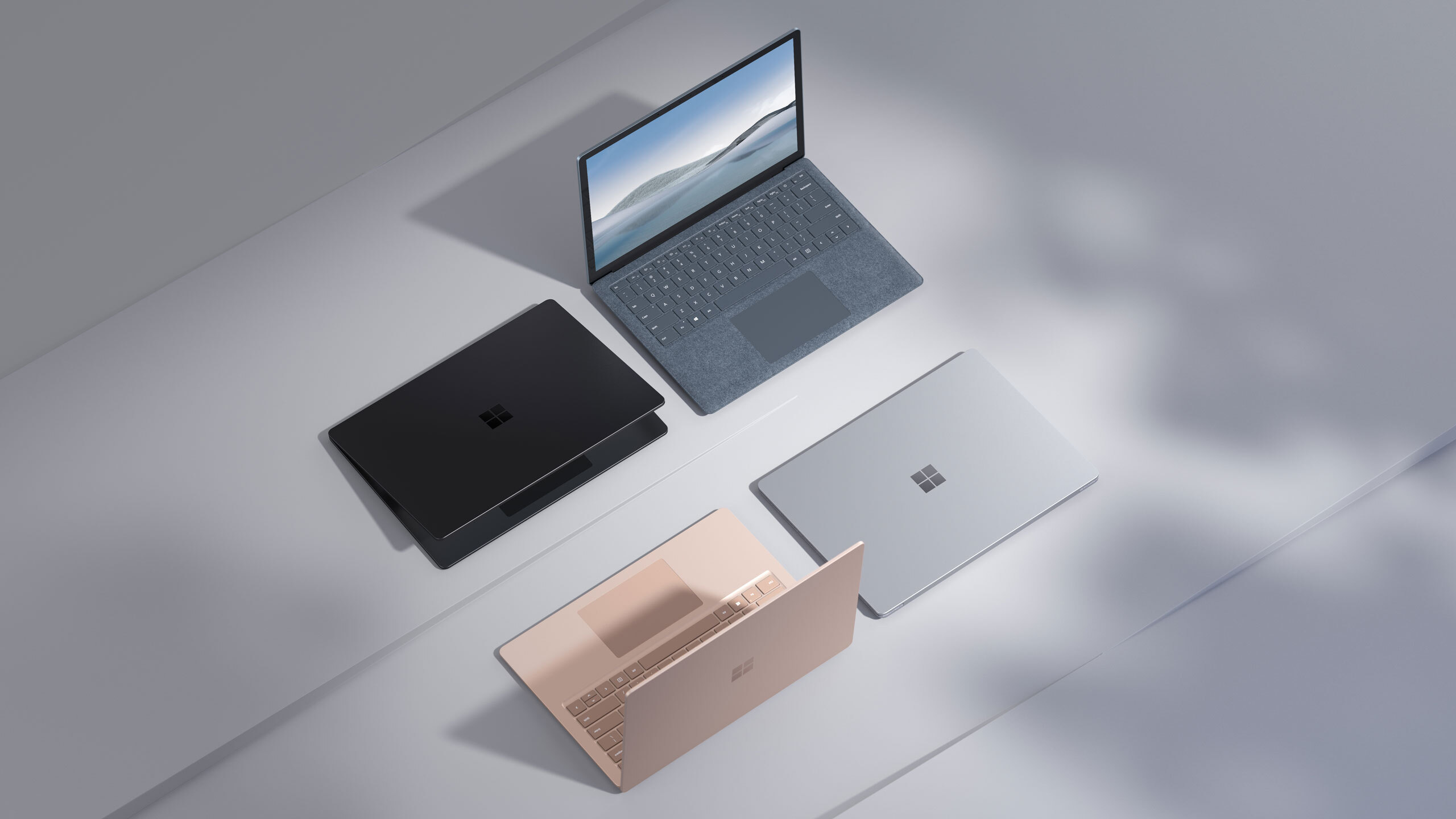
Microsoft today announced the next iteration of its Surface laptop, the Surface Laptop 4. It will start at $999 when it goes on sale on April 15. Perhaps its biggest selling point is choice, with options for both 11th Gen Intel Core processors or an 8-core AMD Ryzen (again called the Microsoft Surface Edition).
Both the 13.5-inch and 15-inch version of the Surface Laptop 4 will offer Intel and AMD options. This is a change from the Surface Laptop 3, which offered Intel in the 13.5-incher and
AMD in the 15-incher
(with the exception of business models).
Microsoft Surface Laptop 4 (13.5-inches)
Microsoft Surface Laptop 4 (15-inches)
CPU
Up to AMD Ryzen Microsoft Surface Edition R5 4680U (8 cores), Up to Intel Core i7-1185G7
Up to AMD Ryzen Microsoft Surface Edition R7 4980U ( 8 cores), Up to Intel Core i7-1185G7
Graphics
AMD Radeon RX Graphics or Intel Xe Graphics
AMD Radeon RX Graphics or Intel Xe Graphics
RAM
Up to 16GB (AMD), Up to 32GB (Intel), LPDDR4X 3,733 MHz
Up to 16GB (AMD, DDR4, 2,400 MHz), up to 32GB (Intel, LPDDR4, 3,733 MHz)
Storage
Up to 256GB (AMD), Up to 1TB (Intel)
Up to 512GB (AMD), Up to 1TB (Intel)
Display
13.5-inch PixelSense display, 2256 x 1504, 3:2
15-inch PixelSense display, 2496 x 1664, 3:2
Networking
Wi-Fi 6 (802.11ax), Bluetooth 5.0
Wi-Fi 6 (802.11ax), Bluetooth 5.0
Starting Price
$999 (AMD), $1,299 (Intel)
$1,299 (AMD), $1,799 (Intel)
The design of the Surface Laptop 4 is largely unchanged, with a 3:2 touchscreen display with 201 pixels per inch, options for Alcantara fabric or a metal deck. There is, however, one new color, ice blue, which debuted on the Surface Laptop Go last year.
Image 1 of 2
(Image credit: Microsoft)
Image 2 of 2
(Image credit: Microsoft)
Many of the biggest changes can’t be seen. For the first time, Microsoft is offering a 32GB RAM option on the Surface Laptop (with an Intel Core i7 at 1TB of RAM on both sizes). The company is claiming up to 19 hours of battery life on the smaller device with an AMD Ryzen 5 or 17 hours with a Core i7. On the bigger size, it’s suggesting up to 17.5 hours with an AMD Ryzen 7 and 16.5 hours with Intel Core i7. Microsoft is also claiming a 70% performance increase, though it doesn’t say with which processor.
The new AMD Ryzen Microsoft Surface Edition chips are based on Ryzen 4000 and Zen 2, rather than Ryzen 5000 and Zen 3, which is just rolling onto the market. We understand Microsoft’s chips are somewhat customized, including frequencies similar to the newer chips. But these new processors should, in theory, lead to increased stability and battery life.
While Microsoft is being more flexible on allowing both Intel and AMD options on both size machines, you won’t find them with identical specs when it comes to RAM and storage. The 13.5-inch laptop will offer Ryzen 5 with 8GB or 16GB of RAM and 256GB of storage, while the Intel 11th Gen Core process range will include a Core i5/8GB RAM/512GB SSD option to start, as well as both Core i5 and Core i7 models with 16GB of RAM and 512GB of storage and a maxxed out version with a Core i7, 32GB of RAM and 1TB storage drive. The Ryzzen versions only come in platinum, while all but the top-end Intel model also include ice blue, sandstone and black.
Image 1 of 2
(Image credit: Microsoft)
Image 2 of 2
(Image credit: Microsoft)
On the 15-inch model, you can get a Ryzen 7 with 8GB of RAM and either 256GB or 512GB of storage, or an R7 with 16GB of memory and a 512GB SSD. For intel, You can choose between an Intel Core i7 with either 16GB of memory and 512GB of storage or 32GB of memory and 1TB of storage. These only come in platinum and black.
Commercial models will add more configurations for businesses, including a 13.5-inch model with 512GB of storage and a Ryzen processor. Overall, there are a lot of configurations, so hopefully people are able to find what they want. But there are definitely more options on the Intel side of the Surface fence.
The port situation is largely the same as last year, including USB Type-A, USB Type-C, a headphone jack and the Surface Connect port. Microsoft still isn’t going with Thunderbolt, and will be using USB-C 3.1 Gen 2 on both the Intel and AMD models. The replaceable SSD is back, though Microsoft continues to state that it isn’t user serviceable, and that it should only be removed by authorized technicians.
It’s been a long wait for the Surface Laptop 4. The Surface Laptop 3 was introduced at an event in October 2019 and went on sale that November. Last year, Microsoft revealed the cheaper, smaller Surface Laptop Go but didn’t update the flagship clamshell. We’ll go hands on with the Surface Laptop 4, so let’s hope the wait was worth it.
Microsoft is also revealing a slew of accessories designed for virtual work. They include the $299.99 Surface Headphones 2+ for Business, which is certified for Microsoft Teams with a dongle, shipping this month; Microsoft Modern USB and wireless headsets ($49.99 and $99.99, respectively, releasing in June); the Microsoft Modern USB-C Speaker ($99.99, releasing in June); and the Microsoft Modern webcam, a $69.99 camera with 1080p video, HDR and a 78-degree field of view that will go on sale in June.
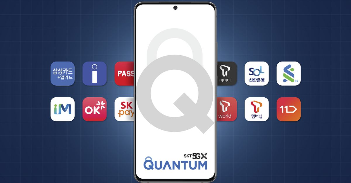
Samsung and South Korean carrier SK Telecom have announced the Galaxy Quantum 2, Samsung’s second phone that features built-in quantum cryptography technology for increased security. It’s the follow-up to last year’s Galaxy A Quantum.
The Quantum 2 includes a chip developed by a company called ID Quantique, which says it’s the world’s smallest quantum random number generator (QRNG) at 2.5mm square. It works by capturing random noise with an LED and a CMOS image sensor. According to SK Telecom, the QRNG chip “allows smartphone holders to use services that require security in a more safe and secure manner by generating unpredictable and patternless true random numbers.”
Quantum cryptography RNG is considered to be extremely challenging to hack without extensive physical access to a given device. The benefits will seem pretty niche to the average customer, but the QRNG chip does automatically work with apps that use the Android Keystore APIs, which should make the technology more accessible for developers. SK Telecom is touting local compatibility with the likes of Shinhan Bank and Standard Chartered Bank Korea, plus its own services like T World. The carrier says it’ll work with more services in the future, including Samsung’s own credit cards.
The phone itself has reasonably high specs, close to what you’d have found in a high-end flagship phone from a year or two ago. It has a Qualcomm Snapdragon 855 Plus processor, a 64-megapixel camera, and a 6.7-inch 120Hz OLED display.
The Galaxy Quantum 2 is only confirmed for a release in South Korea right now. It’ll go on sale on April 23rd.
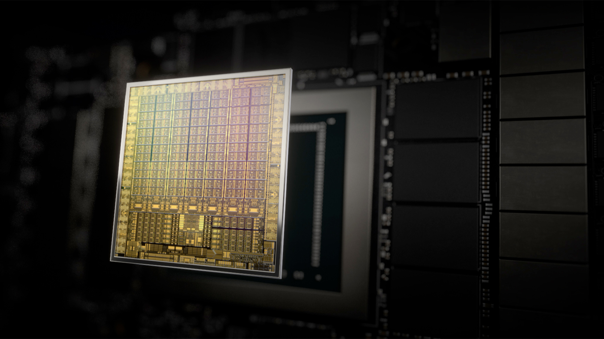
Nvidia’s flagship A100 compute GPU introduced last year delivers leading-edge performance required by cloud datacenters and supercomputers, but the unit is way too powerful and expensive for more down-to-earth workloads. So today at GTC the company introduced two younger brothers for its flagship, the A30 for mainstream AI and analytics servers, and the A10 for mixed compute and graphics workloads.
Comparison of Nvidia’s A100-Series Datacenter GPUs
A100 for PCIe
A30
A10
FP64
9.7 TFLOPS
5.2 TFLOPS
–
FP64 Tensor Core
19.5 TFLOPS
10.3 TFLOPS
–
FP32
19.5 TFLOPS
10.3 TFLOPS
31.2 TFLOPS
TF32
156 TF
82 TF
62.5 TFLOPS
Bfloat16
312 TF
165 TF
125 TF
FP16 Tensor Core
312 TF
165 TF
125 TF
INT8
624 TOPS
330 TOPS
250 TOPS
INT4
1248 TOPS
661 TOPS
500 TOPS
RT Cores
–
–
72
Memory
40 GB HBM2
24 GB HBM2
24 GB GDDR6
Memory Bandwidth
1,555 GB/s
933 GB/s
600 GB/s
Interconnect
12 NVLinks, 600 GB/s
? NVLinks, 200 GB/s
–
Multi-Instance
7 MIGs @ 5 GB
4 MIGs @ 6 GB
–
Optical Flow Acceleration
–
1
–
NVJPEG
–
1 decoder
?
NVENC
–
?
1 encoder
NVDEC
–
4 decoders
1 decoder (+AV1)
Form-Factor
FHFL
FHFL
FHFL
TDP
250W
165W
150W
The Nvidia A30: A Mainstream Compute GPU for AI Inference
Nvidia’s A30 compute GPU is indeed A100’s little brother and is based on the same compute-oriented Ampere architecture. It supports the same features, a broad range of math precisions for AI as well as HPC workloads (FP64, FP64TF, FP32, TF32, bfloat16, FP16, INT8, INT4), and even multi-instance GPU (MIG) capability with 6GB instances. From a performance point of view, the A30 GPU offers slightly more than 50% of A100’s performance, so we are talking about 10.3 FP32 TFLOPS, 5.2 FP64 TFLOPS, and 165 FP16/bfloat16 TFLOPS.
(Image credit: Nvidia)
When it comes to memory, the unit is equipped with 24GB of DRAM featuring a 933GB/s bandwidth (we suspect Nvidia uses three HBM2 stacks at around 2.4 GT/s, but the company has not confirmed this). The memory subsystem seems to lack ECC support, which might be a limitation for those who need to work with large datasets. Effectively, Nvidia wants these customers to use its more expensive A100.
Nvidia traditionally does not disclose precise specifications of its compute GPU products at launch, yet we suspect that the A30 is exactly ‘half’ of the A100 with 3456 CUDA cores, though this is something that is unconfirmed at this point.
Nvidia’s A30 comes in a dual-slot full-height, full length (FHFL) form-factor, with a PCIe 4.0 x16 interface and a 165W TDP, down from 250W in case of the FHFL A100. Meanwhile, the A30 supports one NVLink at 200 GB/s (down from 600 GB/s in case of the A100).
The Nvidia A10: A GPU for AI, Graphics, and Video
Nvidia’s A10 does not derive from compute-oriented A100 and A30, but is an entirely different product that can be used for graphics, AI inference, and video encoding/decoding workloads. The A10 supports FP32, TF32, blfoat16, FP16, INT8 and INT4 formats for graphics and AI, but does not support FP64 required for HPC.
(Image credit: Nvidia)
The A10 is a single-slot FHFL graphics card with a PCIe 4.0 x16 interface that will be installed into servers running the Nvidia RTX Virtual Workstation (vWS) software and remotely powering workstations that need both AI and graphics capabilities. To a large degree, the A10 is expected to be a remote workhorse for artists, designers, engineers, and scientists (who do not need FP64).
Nvidia’s A10 seems to be based on the GA102 silicon (or its derivative), but since it supports INT8 and INT4 precisions, we cannot be 100% sure that this is physically the same processor that powers Nvidia’s GeForce RTX 3080/3090 and RTX A6000 cards. Meanwhile, performance of the A10 (31.2 FP32 TFLOPS, 125 FP16 TFLOPS) sits in the range of the GeForce RTX 3080. The card comes equipped with 24GB of GDDR6 memory offering a 600GB/s bandwidth, which appears to be the memory interface width of the RTX 3090 but without the GDDR6X clock speeds (or power or temperatures).
Pricing and Availability
Nvidia expects its partners to start offering machines with its A30 and A10 GPUs later this year.
Nvidia’s annual GPU Technology Conference (GTC) kicks off today at 8:30 a.m. PT. Due to the Covid-19 restrictions, the chipmaker will be holding the event online with over 1,500 sessions, covering a broad spectrum of topics.
It wouldn’t be a GTC without a keynote from Jensen Huang, which the CEO will deliver from his kitchen again. Don’t forget that Nvidia is still hosting its GTC 2021 treasure hunt, where the ultimate spoil is the $1,499 GeForce RTX 3090. The graphics card shortage isn’t letting up anytime soon so this could be a good opportunity to get your hands on Nvidia’s flagship Ampere graphics card for free.
GTC doesn’t focus on gaming, rather more complex subjects, such as AI, deep learning, quantum computing, or telecommunications – just to mention a few. So we don’t expect Nvidia to launch any new GeForce gaming graphics cards to shake up the best graphics cards on the market. However, we might witness a few Quadro or Tesla announcements.
GTC 2021 runs from April 12 to April 16. Registration is free, and you’ll get access to all the tech sessions, panels and demos. However, if you’re interested in a particular DLI training workshop, it’s priced at $249 each.
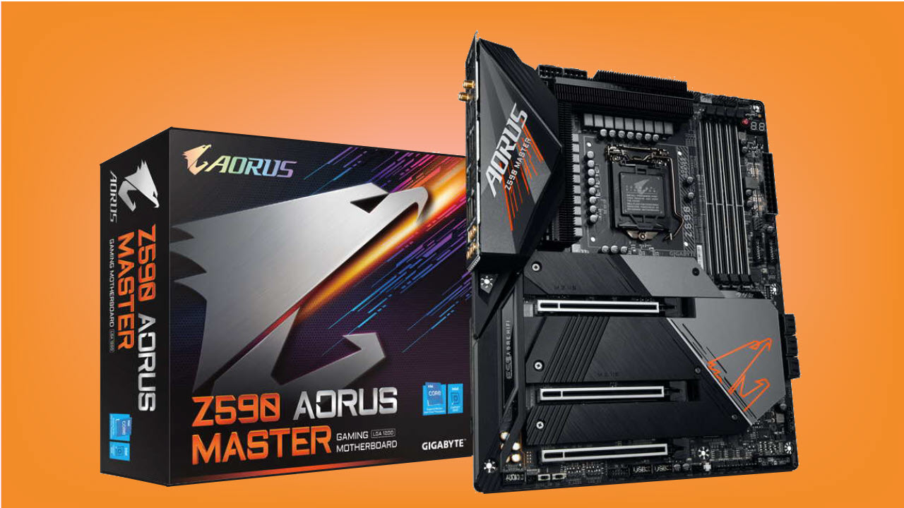
Gigabyte’s Aorus Z590 Master is a well-rounded upper mid-range motherboard with a VRM rivaled by boards that cost twice as much. Between the Wi-Fi 6E and 10 GbE, three M.2 sockets and six SATA ports for storage, plus its premium appearance, the Z590 Master is an excellent option to get into the Z590 platform if you’re willing to spend around $400.
For
+ Fast Networking, Wi-Fi 6E/10 GbE
+ Superior 18-phase 90A VRM
+ 10 USB ports
Against
– No PCIe x1 slot(s)
– Audible VRM fan
– Price
Features and Specifications
Editor’s Note: A version of this article appeared as a preview before we had a Rocket Lake CPU to test with Z590 motherboards. Now that we do (and Intel’s performance embargo has passed), we have completed testing (presented on page 3) with a Core i9-11900K and have added a score and other elements (as well as removing some now-redundant sentences and paragraphs) to make this a full review.
Gigabyte’s Z590 Aorus Master includes an incredibly robust VRM, ultra-fast Wi-Fi and wired networking, premium audio, and more. While its price of roughly $410 is substantial, it’s reasonable for the features you get, and far from the price of the most premium models in recent generations. If you don’t mind a bit of audible VRM fan noise and like lots of USB and fast wired and wireless networking, it’s well worth considering.
Gigabyte’s current Z590 product stack consists of 13 models. There are familiar SKUs and a couple of new ones. Starting with the Aorus line, we have the Aorus Xtreme (and potentially a Waterforce version), Aorus Master, Aorus Ultra, and the Aorus Elite. Gigabyte brings back the Vision boards (for creators) and their familiar white shrouds. The Z590 Gaming X and a couple of boards from the budget Ultra Durable (UD) series are also listed. New for Z590 is the Pro AX board, which looks to slot somewhere in the mid-range. Gigabyte will also release the Z590 Aorus Tachyon, an overbuilt motherboard designed for extreme overclocking.
On the performance front, the Gigabyte Z590 Aorus Master did well overall, performing among the other boards with raised power limits. There wasn’t a test where it did particularly poorly, but the MS Office and PCMark tests on average were slightly higher than most. Overall, there is nothing to worry about when it comes to stock performance on this board. Overclocking proceeded without issue as well, reaching our 5.1 GHz overclock along with the memory sitting at DDR4 4000.
The Z590 Aorus Master looks the part of a premium motherboard, with brushed aluminum shrouds covering the PCIe/M.2/chipset area. The VRM heatsink and its NanoCarbon Fin-Array II provide a nice contrast against the smooth finish on the board’s bottom. Along with Wi-Fi 6E integration, it also includes an Aquantia based 10GbE, while most others use 2.5 GbE. The Aorus Master includes a premium Realtek ALC1220 audio solution with an integrated DAC, three M.2 sockets, reinforced PCIe and memory slots and 10 total USB ports, including a rear USB 3.2 Gen2x2 Type-C port. We’ll cover those features and much more in detail below. But first, here are full the specs from Gigabyte.
Specifications – Gigabyte Z590 Aorus Master
Socket
LGA 1200
Chipset
Z590
Form Factor
ATX
Voltage Regulator
19 Phase (18+1, 90A MOSFETs)
Video Ports
(1) DisplayPort v1.2
USB Ports
(1) USB 3.2 Gen 2×2, Type-C (20 Gbps)
(5) USB 3.2 Gen 2, Type-A (10 Gbps)
(4) USB 3.2 Gen 1, Type-A (5 Gbps)
Network Jacks
(1) 10 GbE
Audio Jacks
(5) Analog + SPDIF
Legacy Ports/Jacks
✗
Other Ports/Jack
✗
PCIe x16
(2) v4.0 x16, (x16/x0 or x8/x8
(1) v3.0 x4
PCIe x8
✗
PCIe x4
✗
PCIe x1
✗
CrossFire/SLI
AMD Quad GPU Crossfire and 2-Way Crossfire
DIMM slots
(4) DDR4 5000+, 128GB Capacity
M.2 slots
(1) PCIe 4.0 x4 / PCIe (up to 110mm)
(1) PCIe 3.0 x4 / PCIe + SATA (up to 110mm)
(1) PCIe 3.0 x4 / PCIe + SATA (up to 110mm)
U.2 Ports
✗
SATA Ports
(6) SATA3 6 Gbps (RAID 0, 1, 5 and 10)
USB Headers
(1) USB v3.2 Gen 2 (Front Panel Type-C)
(2) USB v3.2 Gen 1
(2) USB v2.0
Fan/Pump Headers
(10) 4-Pin
RGB Headers
(2) aRGB (3-pin)
(2) RGB (4-pin)
Legacy Interfaces
✗
Other Interfaces
FP-Audio, TPM
Diagnostics Panel
Yes, 2-character debug LED, and 4-LED ‘Status LED’ display
As we open up the retail packaging, along with the board, we’re greeted by a slew of included accessories. The Aorus Master contains the basics (guides, driver CD, SATA cables, etc.) and a few other things that make this board complete. Below is a full list of all included accessories.
Installation Guide
User’s Manual
G-connector
Sticker sheet / Aorus badge
Wi-Fi Antenna
(4) SATA cables
(3) Screws for M.2 sockets
(2) Temperature probes
Microphone
RGB extension cable
Image 1 of 3
(Image credit: Gigabyte)
Image 2 of 3
(Image credit: Gigabyte)
Image 3 of 3
(Image credit: Gigabyte)
After taking the Z590 Aorus Master out of the box, its weight was immediately apparent, with the shrouds, heatsinks and backplate making up the majority of that weight. The board sports a matte-black PCB, with black and grey shrouds covering the PCIe/M.2 area and two VRM heatsinks with fins connected by a heatpipe. The chipset heatsink has the Aorus Eagle branding lit up, while the rear IO shroud arches over the left VRM bank with more RGB LED lighting. The Gigabyte RGB Fusion 2.0 application handles RGB control. Overall, the Aorus Master has a premium appearance and shouldn’t have much issue fitting in with most build themes.
(Image credit: Gigabyte)
Looking at the board’s top half, we’ll first focus on the VRM heatsinks. They are physically small compared to most boards, but don’t let that fool you. The fin array uses a louvered stacked-fin design Gigabyte says increases surface area by 300% and improves thermal efficiency with better airflow and heat exchange. An 8mm heat pipe also connects them to share the load. Additionally, a small fan located under the rear IO shroud actively keeps the VRMs cool. The fan here wasn’t loud, but was undoubtedly audible at default settings.
We saw a similar configuration in the previous generation, which worked out well with an i9-10900K, so it should do well with the Rocket Lake flagship, too. We’ve already seen reports indicating the i9-11900K has a similar power profile to its predecessor. Feeding power to the VRMs is two reinforced 8-pin EPS connectors (one required).
To the right of the socket, things start to get busy. We see four reinforced DRAM slots supporting up to 128GB of RAM. Oddly enough, the specifications only list support up to DDR4 3200 MHz, the platform’s limit. But further down the webpage, it lists DDR4 5000. I find it odd it is listed this way, though it does set up an expectation that anything above 3200 MHz is overclocking and not guaranteed to work.
Above the DRAM slots are eight voltage read points covering various relevant voltages. This includes read points for the CPU Vcore, VccSA, VccIO, DRAM, and a few others. When you’re pushing the limits and using sub-ambient cooling methods, knowing exactly what voltage the component is getting (software can be inaccurate) is quite helpful.
Above those on the top edge are four fan headers (next to the EPS connectors is a fifth) of 10. According to the manual, all CPU fan and pump headers support 2A/24W each. You shouldn’t have any issues powering fans and a water cooling pump. Gigabyte doesn’t mention if these headers use auto-sensing (for DC or PWM control), but they handled both when set to ‘auto’ in the BIOS. Both a PWM and DC controlled fan worked without intervention.
The first two (of four) RGB LED headers live to the fan headers’ right. The Z590 Aorus Master includes two 3-pin ARGB headers and two 4-pin RGB headers. Since this board takes a minimal approach to RGB lighting, you’ll need to use these to add more bling to your rig.
We find the power button and 2-character debug LED for troubleshooting POST issues on the right edge. Below is a reinforced 24-pin ATX connector for power to the board, another fan header and a 2-pin temperature probe header. Just below all of that are two USB 3.2 Gen1 headers and a single USB 3.2 Gen2x2 Type-C front-panel header for additional USB ports.
(Image credit: Tom’s Hardware)
Gigabyte chose to go with a 19-phase setup for the Vcore and SOC on the power delivery front. Controlling power is an Intersil ISL6929 buck controller that manages up to 12 discrete channels. The controller then sends the power to ISL6617A phase doublers and the 19 90A ISL99390B MOSFETs. This is one of the more robust VRMs we’ve seen on a mid-range board allowing for a whopping 1,620A available for the CPU. You won’t have any trouble running any compatible CPU, including using sub-ambient overclocking.
(Image credit: Gigabyte)
The bottom half of the board is mostly covered in shrouds hiding all the unsightly but necessary bits. On the far left side, under the shrouds, you’ll find the Realtek ALC1220-VB codec along with an ESS Sabre ESS 9118 DAC and audiophile-grade WIMA and Nichicon Fine Gold capacitors. With the premium audio codec and DAC, an overwhelming majority of users will find the audio perfectly acceptable.
We’ll find the PCIe slots and M.2 sockets in the middle of the board. Starting with the PCIe sockets, there are a total of three full-length slots (all reinforced). The first and second slots are wired for PCIe 4.0, with the primary (top) slot wired for x16 and the bottom maxes out at x8. Gigabyte says this configuration supports AMD Quad-GPU Cand 2-Way Crossfire. We didn’t see a mention of SLI support even though the lane count supports it. The bottom full-length slot is fed from the chipset and runs at PCIe 3.0 x4 speeds. Since the board does without x1 slots, this is the only expansion slot available if you’re using a triple-slot video card. Anything less than that allows you to use the second slot.
Hidden under the shrouds around the PCIe slots are three M.2 sockets. Unique to this setup is the Aorus M.2 Thermal Guard II, which uses a double-sided heatsink design to help cool M.2 SSD devices with double-sided flash. With these devices’ capacities rising and more using flash on both sides, this is a good value-add.
The top socket (M2A_CPU) supports up to PCIe 4.0 x4 devices up to 110mm long. The second and third sockets, M2P_SB and M2M_SB, support both SATA and PCIe 3.0 x3 modules up to 110mm long. When using a SATA-based SSD on M2P_SB, SATA port 1 will be disabled. When M2M_SB (bottom socket) is in use, SATA ports 4/5 get disabled.
To the right of the PCIe area is the chipset heatsink with the Aorus falcon lit up with RGB LEDs from below. There’s a total of six SATA ports that support RAID0, 1, 5 and 10. Sitting on the right edge are two Thunderbolt headers (5-pin and 3-pin) to connect to a Gigabyte Thunderbolt add-in card. Finally, in the bottom-right corner is the Status LED display. The four LEDs labeled CPU, DRAM, BOOT and VGA light up during the POST process. If something hangs during that time, the LED where the problem resides stays lit, identifying the problem area. This is good to have, even with the debug LED at the top of the board.
Across the board’s bottom are several headers, including more USB ports, fan headers and more. Below is the full list, from left to right:
Front-panel audio
BIOS switch
Dual/Single BIOS switch
ARGB header
RGB header
TPM header
(2) USB 2.0 headers
Noise sensor header
Reset button
(3) Fan headers
Front panel header
Clear CMOS button
(Image credit: Gigabyte)
The Z590 Aorus Master comes with a pre-installed rear IO panel full of ports and buttons. To start, there are a total of 10 USB ports out back, which should be plenty for most users. You have a USB 3.2 Gen2x2 Type-C port, five USB 3.2 Gen2 Type-A ports and four USB 3.2 Gen1 Type-A ports. There is a single DisplayPort output for those who would like to use the CPU’s integrated graphics. The audio stack consists of five gold-plated analog jacks and a SPDIF out. On the networking side is the Aquantia 10 GbE port and the Wi-Fi antenna. Last but not least is a Clear CMOS button and a Q-Flash button, the latter designed for flashing the BIOS without a CPU.
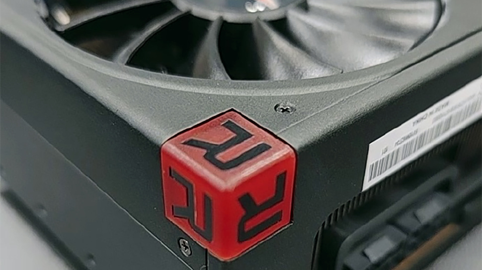
A Lenovo product manager has published the first pictures of its upcoming Radeon RX 6900 XT Legion graphics card. The board looks as monumental as the renders released a few months ago, and the very emergence of the photos may indicate that the product is close to release.
Lenovo’s Radeon RX 6900 XT Legion carries AMD’s flagship Navi 21 GPU in its maximum configuration with 5120 stream processors as well as 16 GB of GDDR6 memory connected to the chip using a 256-bit interface. Just like AMD’s reference cards, it has two eight-pin auxiliary PCIe power connectors. That means Lenovo isn’t going after extreme factory overclocking for this board, unlike traditional add-in-board (AIB) makers that install three eight-pin power connectors on their custom Radeon RX 6900 XT products.
(Image credit: WolStame/Weibo)
The AIB presumably uses a proprietary printed circuit board (PCB) and comes equipped with a massive triple-slot cooling system featuring three fans that resemble a cooler used on reference AMD Radeon VII graphics cards several years ago.
Meanwhile, to appeal to modern enthusiasts, Lenovo equipped its cooling system with RGB LEDs that highlight the Radeon RX 6900 XT model on top and the Legion brand on the back. Also, there is a highlighted ‘R’ located on one edge of the card.
(Image credit: WolStame/Weibo)
The graphics card was pictured by WolStame, who happens to be a Lenovo China Gaming Desktop Product Planning Manager (according to VideoCardz), and published on his Weibo page. WolStame said that the AIB is an engineering sample, though it looks rather solid.
(Image credit: WolStame/Weibo)
At this point, it is still unclear whether Lenovo will use its Radeon RX 6900 XT graphics cards exclusively with its Savior Blade 7000P 2021 gaming PCs or will also sell them separately, just like it does with its Legion-branded monitors and other gear. After all, what’s the point of developing an exclusive graphics card for just one PC?
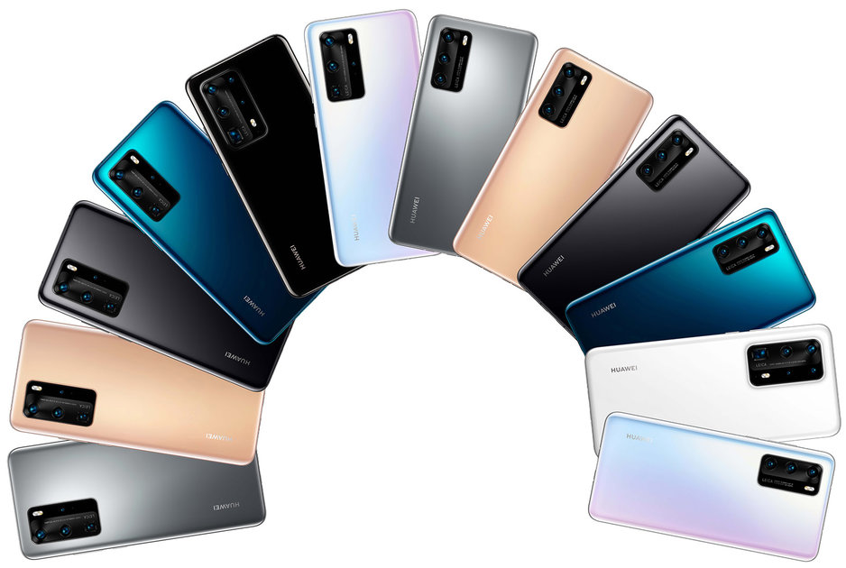
(Pocket-lint) – Not content with bringing its usual two-model flagship series release programme, for 2020 Huawei stepped things up by bringing not just one, not two, but three different P series handsets: the P40, the P40 Pro, and the P40 Pro+.
It’s a move that came as no surprise, in a world where many competitors have gone down a similar route – check out Samsung’s S20 series, for example – but with now three P40 series models to choose from, just how do they differ?
squirrel_widget_203929
Design: Colours & Finishes
P40 Pro only: Silver Frost, Blush Gold with matte-touch finish
P40 Pro+ only: Black ceramic, White ceramic
All models: Ice White, Black, DeepSea Blue
The standard P40 is smaller than the P40 Pro and Pro+, the latter two are the very same size.
But the colour options and finishes is where things differ. At the entry point there’s white, black and blue glass-backed finishes. The P40 Pro also options a silver and pink-gold finish, both of which have a matte-touch finish which is said to be fingerprint repellent – despite still being made of glass.
Lastly there’s a ceramic finish, in either black or white, for the P40 Pro+ only. Huawei tells us this “nanotech ceramic back” is comprised of ceramic beads, which are compressed at higher pressure, then kilned at 1500C for five days, creating a sapphire-strength rear with a reflective index “similar to diamond”.
Screen: Size & Resolution
P40 Pro & Pro+: Edge-to-edge ‘Overflow Display’ with curved edges / P40: Flat display
P40 Pro & Pro+: 6.58-inch OLED, 2640 x 1200 resolution
P40: 6.1-inch OLED, 2340 x 1080 resolution
P40 Pro & Pro+: 90Hz / P40: 60Hz
As we said, the P40 is the smaller handset, on account of its 6.1-inch screen. This display is also flat, not curved, with slightly larger bezels than its bigger models.
The P40 Pro and Pro+ have a 6.58-inch screen, so aren’t as ultra-massive as some current handsets, such as the Samsung Galaxy S21 Ultra. We think that’s a sensible decision, to make for greater ease of use with one hand.
Whichever of the Pro and Pro+ models you choose you’ll be getting a so-called ‘Overflow Display’. That’s Huawei’s way of saying Waterfall Display, really, meaning the edges spill over, much like a waterfall, so the edge bezel is barely visible. This applies to all edges – both sides and the top and the bottom – for a real screen-dominant design.
There’s no notch as a result, instead a dual punch-hole is present on all three handsets. More info about the (extensive!) cameras is further down the page.
While the P40 offers a standard 60Hz display, the Pro and Pro+ offer a 90Hz refresh rate – which is 50 per cent greater than the typical 60Hz panels. That’s all well and good, but with OnePlus running 120Hz panels and others offering up to 165Hz panels in gaming phones (the Red Magic 6 the first example of that), you might wonder why Huawei hasn’t reached to the stars here. The answer, we suspect, is cost, battery performance, and, frankly, that this extra rate won’t make a huge difference in the way most people see apps and content perform anyway.
Performance
All models: Kirin 990 processor, 8GB RAM
P40 Pro & Pro+: 4,200mAh battery
P40: 3,800mAh battery
P40 Pro+: 40W fast-charging (incl. 40W wireless)
P40 Pro: 40W fast-charging (incl. 27W wireless)
P40: 22.5W fast-charging (no wireless charging)
All three P40 models will deliver a similar experience, given their Kirin 990 processor, 8GB RAM, and 5G connectivity across the board.
None of the three will come with Google Services, though, which means no access to Google Play Store (instead there’s Huawei’s App Gallery, which lacks some of the majors at present, such WhatsApp (you can download it as an APK using a browser though – but no Google Drive will mean no backup), and more. That’s despite the P40 launching on Google’s Android 10 operating system, with Huawei’s EMUI 10.1 user interface.
What apps can you actually get on Huawei’s App Gallery?
It’s in the battery department where the three models differ a little more. The P40 has a 3,800mAh cell, which is fairly small by today’s standards, while the Pro and Pro+ up that to 4,200mAh – which is about on par with what current competitors offers.
The recharging of those batteries is speedy too. The P40 sticks to the well-established 22.5W fast-charging, while the P40 Pro and Pro+ up this to 40W – which is quick, but not the very fastest available (that goes to OnePlus with its 65W Warp Charge 65T for the OnePlus 9 Pro).
However, Huawei is introducing 40W wireless charging to the Pro+. It means wire-free charging of the handset in little more than an hour – which is impressive. The standard P40, however, has no wireless charging capability.
Cameras
P40: Leica triple camera system
P40 Pro: Leica quad camera system
P40 Pro+: Leica penta camera system
Main camera:
All models: 50MP SuperSensing (RYYB) sensor, 1/1.28in size
f/1.9 aperture, optical stabilisation (OIS)
Focal length (approx): P40 at 27mm, Pro at 25mm, Pro+ at 24mm
Ultra-wide camera:
P40: 16MP, f/2.2, 17mm equiv.
P40 Pro & Pro+: 40MP cine lens, f/1.8, 18mm equiv.
Always the P series’ big-hitting feature is its camera setup. We thought the P30 Pro set a new bar when it launched in 2019 – something that the P40 series bettered.
It’s a little complicated, though, as the camera setup for each device is rather different. The P40 has a triple camera rear, the P40 Pro a quad setup, the Pro+ a penta system.
However, all three offer one consistent thing: the same main camera. This is a 50-megapixel SuperSensing sensor – the same red, yellow, blue (RYYB) technology as in the P30 Pro – and, at 1/1.28in size, it’s a lot larger than a typical camera sensor.
That make-up and physical size work to its benefit in delivering a clean signal for better image quality overall. Not to mention the use of four pixels into one on-screen pixel means oversampling for even better quality (12.5MP output) – a method used by many others already. And there’s 100 per cent on-sensor phase-detection pixels for autofocus too.
There’s a wide-angle camera on each P40 model, too, but it’s one of two variants: the P40 has a 16-megapixel sensor at a 17mm focal length, while the Pro and Pro+ offer 40MP at 18mm (so it’s slightly less wide, likely for the sake of edge/corner quality). The higher-resolution offering is described as a ‘cine lens’ as it’s also used to cater for video, at up to 4K.
Then there’s the zoom element. All three P40 models have an optical zoom lens: the P40 a 3x zoom, the P40 Pro a 5x zoom, the P40 Pro+ a 10x zoom. That 3x is the same as we’ve seen in the P30, with just 8-megapixels of resolution for the P40 and P40 Pro+. The 5x is different to the one found in the P30 Pro, as Huawei is also utilising the RYYB SuperSensing technology here for the P40 Pro’s zoom. The 10x was the first time we’d seen such a periscope zoom, as reserved for the P40 Pro+ only (and used in tandem with the 3x zoom optic to offer the ability to step through zoom levels to deliver the most appropriate tools for each job).
The P40 Pro and Pro+ also come with a Time-of-Flight depth sensor, which derives distance information, which the software can utilise in layers to help create background blur (bokeh) in portrait mode.
All three P40 cameras will offer familiar modes, from Artificial Intelligence shooting, to Night Mode. However, these have been advanced, with the AI tech now able to shoot multiple frames before during and after pressing the shutter to select the best of a burst and suggest a top three selection.
The front cameras can be found in a dual punch-hole or ‘pill’ cut-out in all three P40 models. The main camera is 32-megapixels, which also uses four-in-one oversampling for 8MP output by default, paired with a depth sensor for background blur software effects and more.
squirrel_widget_203940
Price, Release Date & Conclusion
P40: €799 (at launch)
P40 Pro: €999 (at launch)
P40 Pro+: €1399 (at launch)
Once again the P40 series looks to be grappling for camera dominance. And that variety of versatile cameas – especially on the Pro+ model – make for great reading.
That said, the absence of Google Play Store on these devices is a major pain point. Sure, there’s App Gallery, and consumers have choice in what’s important to them. But, right now, it makes the P40 series difficult to recommend.
In a bid to sell more products to their loyal customers, many of hardware makers these days start offering new product categories. Earlier this year at CES, MSI outlined plans to start offering SSDs under its newly introduced Spatinum brand.
At the time the company only announced its flagship module featuring a PCIe 4.0 x4 interface rated for a 7,000 MB/s read speed as well as a 6.900 MB/s write speed, but it turns out MSI has readied a range of drives.
MSI has registered dozens of Spatinum SSD models with the with the Eurasian Economic Commission (ECC) in a bid to supply them to countries that belong to the Eurasian Economic Union, as discovered by PC Gamer. Not all products registered with the EEC actually reach the market, but at least some of them do. If MSI proceeds with what it registered with the ECC, its choice of drives will include three product families that will all include eight subfamilies, reports ComputerBase:
The Spatinum M400: top-of-the-range SSDs with a PCIe 4.0 interface. Expected to include M480, M471, and M470 models for different sub-segments of the market. Capacities set to range from 500GB to 2TB.
The Spatinum M300: mainstream SSDs with a PCIe 3.0 interface and capacity points from 256GB to 2TB. Projected to feature M381, M380, M371, and M370 model ranges.
The Spatinum S200: entry-level drives in a 2.5-inch form-factor with a SATA interface that will start at 240GB and will top at 1TB.
We don’t yet know the specs of MSI’s drives, but typically PC and hardware makers choose to use off-the-shelf designs offered by companies like Phison and Silicon Motion, which reduces risks and allows to quickly roll out a comprehensive product family. MSI has reportedly started to offer its Spatinum M370 drives to its partner CyberPowerPC in the U.S.
Considering that MSI sells not only motherboards, but also desktops, it makes a great sense for the company to also offer a range of SSDs. Meanwhile, it is unlikely that the company will indeed proceed with eight SSD models. When you join the ranks of over 200 SSD suppliers, you’d better keep your product line lean.
HMD is announcing six new midrange devices today led by the Nokia X20, a midrange handset priced starting at €349 / £299.99 (around $415). It will release in “select markets globally” such as the UK starting next month, but we’re still waiting on HMD to confirm exact US pricing and availability. I’ve been using the phone running near-final software over the past week, which has been enough to get some rough first impressions about the device.
To be frank, the Nokia X20 isn’t the most exciting device. But HMD’s promises about ongoing software and hardware support for the phone make it compelling.
The Nokia X20 is specced like a device at this price point is expected to be. It’s powered by a modest Qualcomm Snapdragon 480 processor paired with either 6 or 8GB of RAM (my device has 6GB), 128GB of expandable storage, and a 4,470mAh battery. It’s got a 6.67-inch, 1080p 60Hz display with a small hole-punch notch and four rear cameras including an ultrawide, macro, and depth sensor.
There’s a side-mounted fingerprint sensor on the right of the device.
The company says it’ll provide three years of monthly security updates for the X20 after launch, three years of OS updates, and to ensure the hardware doesn’t give up the ghost before software support ends, it’s also extending its normal manufacturer’s warranty by an extra year. “In the majority of places,” a company spokesperson says, “that extends it to three years.” If all goes to plan, the Nokia X20 should still be under warranty when it receives its Android 14 update.
In the past, HMD has generally been good at updating its phones over time, though ComputerWorld’sAndroid 11 upgrade tracker reports that it’s been more sluggish lately. Recently, HMD updated its Nokia 8.1 and Nokia 3.2, which released in 2018 and 2019, to Android 11 as part of an upgrade roadmap that includes over a dozen of its devices.
Three years of security updates is a little less than the four years Samsung recently said it would offer for its Galaxy devices, but Samsung’s warranty varies between one and two years depending on whether you’re in the US or UK. Apple recently updated its 2015 iPhone 6S to iOS 14 (five years after its release), but its standard limited warranty also typically only covers new phones for between one and two years.
Along with aiming for three years of use, HMD has also made a couple of other decisions with the Nokia X20 in the name of being eco-friendly. First, in the EU it’s joining Apple and others by not including a power brick in the box, just a USB-C cable. What you do get in the box is a 100 percent compostable phone case. It’s a neat idea producing a case that won’t end up in a landfill, but the accessory itself is frustrating to use. The portion of the case that covers the phone’s volume rocker just isn’t flexible enough, making it hard to press the side of the button that I wanted.
The speed and performance of the phone was generally fine, but I saw the occasional hitch while switching quickly between apps, which made me question how this phone will perform after three years of OS updates. Otherwise, I didn’t have any problems with performance in everyday usage. The X20 supports Sub-6GHz 5G, which won’t matter much to you now but could in three years’ time.
You can find a selection of photo samples below, but in my time with the phone I was underwhelmed by the Nokia X20’s camera performance. The phone has a total of four rear cameras: a 64-megapixel main camera, a 5-megapixel ultrawide, a 2-megapixel depth sensor, and a 2-megapixel macro.
HMD Nokia X20, macro camera.
Ultrawide camera.
Performance in daylight is broadly fine, but when things are more dimly lit you quickly start to lose detail and definition. Neither the ultrawide camera nor the macro camera have the resolution to take decent photographs, and the 2-megapixel macro camera in particular is a pointless and puzzling inclusion.
HMD’s Nokia X20 can’t make any big claims about being a flagship hit, but its modest price tag and HMD’s promises about continued support could make it a safe, dependable smartphone if that’s what you’re after.
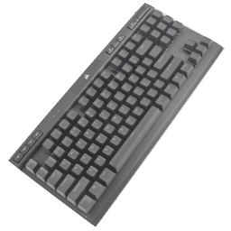
We just had a new CORSAIR keyboard launch a couple of weeks ago, and the company did introduce a few new things with the flagship K100 keyboard late last year, including a standard bottom row of keycaps and stock PBT doubleshot keycaps that necessitated a new mold. Now, anyone with an inkling of how much a keycap set mold costs will tell you that it makes sense to amortize that cost in the form of new products using the same keycap design. Add to this train of thought CORSAIR’s AXON hyper-processing technology, also introduced with the K100, and the likelihood of seeing a revamp of their keyboard lineup sooner rather than later suddenly makes sense. The K65 RGB Mini was a pleasant surprise in the new-to-CORSAIR form factor, however, and then the company gave some love to their membrane keyboard lineup with the K55 RGB PRO (XT). This trend continues with a TKL version of their most popular keyboard that launches today. Thanks again to CORSAIR for sending a review sample of the K70 RGB TKL CHAMPION SERIES keyboard to TechPowerUp!
What do you do when you run out of numbers in your keyboard numbering scheme? CORSAIR thought the answer is to add more verbiage instead. They have done so in the past with such unique descriptors as “STRAFE” or “Silent” and “RAPIDFIRE” for their then-exclusive MX Silent and MX Speed Cherry MX switches. With the all-new K70 RGB TKL, CORSAIR seems to have created a new sub-series called “CHAMPION,” which of course has to be all caps for that sweet SEO. I will henceforth just refer to it as the CORSAIR K70 TKL for the sake of convenience, and know right away that there is more than just a cut-down K70 keyboard here. Sure, they have had TKL keyboards before and continue to do so now, but this is their first smaller-than-full-size keyboard with the same design language as their higher-end aluminium-frame keyboards. Let’s explore all this and more in this review beginning with a look at the specifications below.
Specifications
CORSAIR K70 RGB TKL Keyboard
Layout:
TKL form factor in a US ANSI layout, language support dependent on region
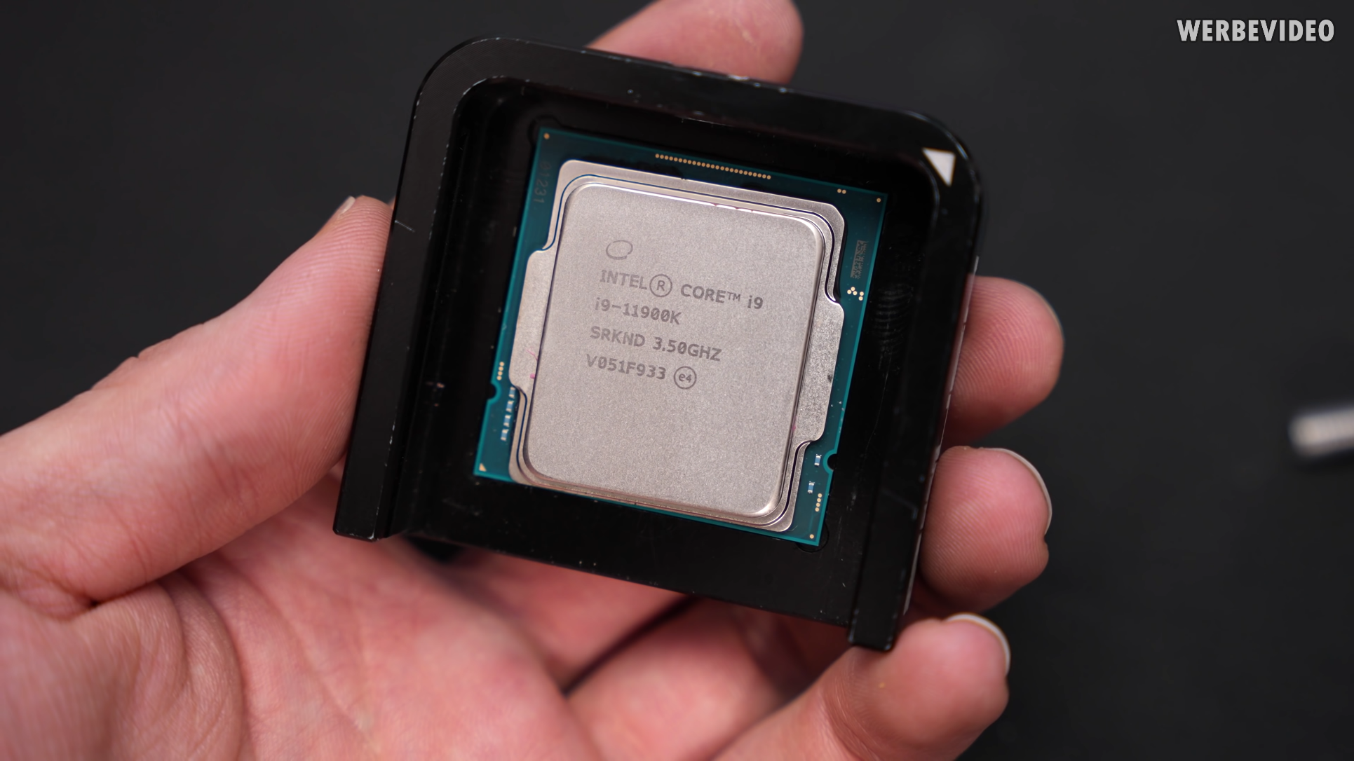
A week ago, German overclocker der8auer published a video showcasing his findings on delidding a Core i9-11900K, Intel’s new flagship Rocket Lake CPU. It’s not one of the best CPUs, based on our testing, but it’s still a formidable opponent in the right workloads. der8auer found that delidding Rocket Lake yielded very impressive temperature results; however, the process is so difficult that it might not be worth the effort.
The problem with the 11900K is its more complex PCB layout of components. Next to the IHS are a bunch of tiny SMD (surface mounted device) capacitors that are incredibly delicate. The capacitors are so close to the IHS that you can easily hit one of them while removing the IHS, which would likely render the CPU nonfunctional.
This is unlike the earlier 9th and 10th Gen chips that don’t have any SMDs anywhere near the IHS, allowing for a (relatively) safe delidding process if you have the right tools. But der8auer is a professional overclocker and skilled at delidding, so he took the chance on his 11900K.
Not only do the SMDs pose problems, but what’s even worse is the amount of pressure you need to apply to the 11900K during the delidding. der8auer had to upgrade his CPU delidding tool with a torque wrench to get the IHS to move at all, where past CPUs only needed an Allen wrench. You can see the strain of trying to twist the tool while keeping the delidding box stable in the above video.
Needless to say, this adds significant risk to the delidding process. Even with the torque wrench, the IHS didn’t want to come off, so der8auer had to resort to warming the CPU up in an oven first. In the end, he was able to successfully remove the IHS, though he mentions several times that he would not recommend most people attempt to do so.
(Image credit: YouTube)
The good news is that the end results are quite impressive. der8uer noted a 10C–12C reduction in temperatures, purely from scraping off the solder on the IHS and replacing it with liquid metal.
This is very impressive on a chip that already has solder. Using solder (as opposed to some form of thermal paste) between the CPU die and the IHS is already a good solution for thermal dissipation. Upgrading to liquid metal normally only results in about a 5C reduction in temperatures, not 10-12C.
It’s rather unfortunate that the delidding process is so incredibly risky on Comet Lake CPUs. We’d love to see more delidded 11900K testing to see if der8auer’s results are typical, but the likelihood of damaging the CPU is so great that it’s not worth the risk for the vast majority of users — even for an impressive 10C drop in temperatures.
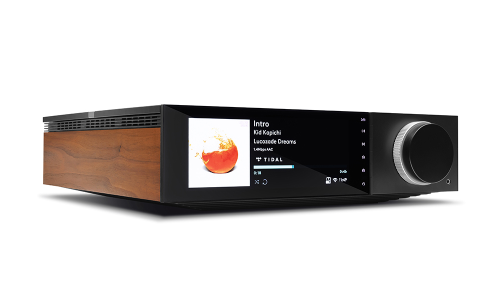
Cambridge Audio has just unleashed two beautiful beasts into the just-add-speakers streaming system market. The Evo 75 and Evo 150 are the first of their kind from the British brand, and oh boy don’t they look lovely?
Hopefully they sound just as lovely too – not least as they’re positioned in the firing line of the multi-Award-winning Naim Uniti Atom and five-star Arcam SA30.
Cambridge is hoping to continue its good run of form with this new product venture, which is naturally based on the company’s established StreamMagic streaming platform for playback over – deep breath – DLNA, AirPlay 2, Bluetooth, Chromecast, Spotify Connect, Tidal Connect, Qobuz, aptX HD Bluetooth and internet radio. The new Evo systems are also Roon Ready.
(Image credit: Cambridge Audio)
The Evo 75 and Evo 150 are powered by Hypex NCore Class D amplifiers (chosen by Cambridge for their, “clear advantages in clarity, resolution and musicality”) and rated at 75 and 150 watts per channel respectively.
The other discrepancy between the two models lies in physical connectivity: both have RCA, optical and coaxial inputs as well as HDMI ARC and 3.5mm headphone sockets, but the Evo 150 expands on that further with an MM phono stage, asynchronous USB and balanced XLR inputs, plus two sets of speaker terminals for running two pairs of speakers. The Evos are determined not to be out-featured.
That walnut wooden panel you see up top is a nod to Cambridge’s first-ever product, the 1968-released P40 amplifier, although owners can choose to dress the black anodised aluminium cabinet with black side panels made from Richlite (an innovative new material made primarily from recycled paper) instead. The side panels can also be switched out according to each customer’s taste.
Completing the look is a dual-concentric rotary dial and 6.8in LCD panel that hark back to the company’s flagship Edge products.
(Image credit: Cambridge Audio)
The Cambridge Audio Evo 75 and Evo 150 will be available from this month, priced £1799 ($2250) and £2249 ($3000) respectively.
A specifically designed Evo CD transport (£799, $950) and a pair of Evo S speakers (£649, $750) will join the Evo range later in the year, with further details on those promised nearer the time.
Whether or not the new Cambridge Evo systems have sonic appeal remains to be heard, but one thing’s for sure: they have plenty of visual appeal.
MORE:
Good news! Tidal Connect comes to Cambridge Audio music streamers
See our pick of the best hi-fi systems 2021: micro, hi-fi, vinyl
Intel last week debuted the 11th Gen Core “Rocket Lake” desktop processor family, and we had launch-day reviews of the Core i9-11900K flagship and the mid-range Core i5-11600K. Today we bring you the Core i5-11400F—probably the most interesting model in the whole stack. The often-ignored SKU among Intel desktop processors among the past many generations, the Core i5-xx400, is also its most popular among gamers. Popular chips of this kind included the i5-8400, the i5-9400F, and the i5-10400F.
These chips feature the entire Core i5 feature-set at prices below $200, albeit lower clock speeds and locked overclocking. Even within these, Intel introduced a sub-segment of chips that lack integrated graphics, denoted by “F” in the model number; which shave a further $15-20 off the price. The Core i5-11400F starts at just $160, which is an impressive value proposition for gamers who use graphics cards and don’t need the iGPU anyway.
The new “Rocket Lake” microarchitecture brings four key changes that make it the company’s first major innovation for client desktop in several years. First, Intel is introducing the new “Cypress Cove” CPU core that promises an IPC gain of up to 19% over the previous-generation. Next up, is the new UHD 750 integrated graphics powered by the Intel Xe LP graphics architecture, promising up to 50% performance uplift over the UHD 650 Gen9.5 iGPU of the previous generation. Thirdly, a much needed update to the processor’s I/O, including PCI-Express 4.0 for graphics and a CPU-attached NVMe slot; and lastly, an updated memory controller that allows much higher memory overclocking potential, thanks to the introduction of a Gear 2 mode.
The Core i5-11400F comes with a permanently disabled iGPU and a locked multiplier. Intel has still enabled support for memory frequencies of up to DDR4-3200, which is now possible on even the mid-tier H570 and B560 motherboard chipsets. The i5-11400F is a 6-core/12-thread processor clocked at 2.60 GHz, with up to 4.40 GHz Turbo Boost frequency. Each of the processor’s six “Cypress Cove” CPU cores include 512 KB dedicated L2 cache, and the cores share 12 MB of L3 cache. Intel is rating the processor’s TDP at 65 W, just like the other non-K SKUs, although it is possible to tweak these power limits—adjusting PL1 and PL2 is not considered “overclocking” by Intel, so it is not locked.
At $170, the Core i5-11400F has no real competitor from AMD. The Ryzen 5 3600 starts around $200, and the company didn’t bother (yet?) with cheaper Ryzen 5 SKUs based on “Zen 3”. In this review, we take the i5-11400F for a spin to show you if this is really all you need for a mid-priced contemporary gaming rig.
We present several data sets in our Core i5-11400F review: “Gear 1” and “Gear 2” show performance results for the processor operating at stock, with the default power limit setting active, respecting a 65 W TDP. Next up we have two runs with the power limit setting raised to maximum: “Max Power Limit / Gear 1” and “Max Power Limit / Gear 2”. Last but not least, signifying the maximum performance you can possible achieve on this CPU, we have a run “Max Power + Max BCLK”, which operates at 102.9 MHz BCLK—the maximum allowed by the processor, at Gear 1 DDR4-3733, the memory controller won’t run higher.
Alienware has announced the latest revision to its flagship gaming laptop lineup, the 15-inch Alienware M15 R5. It’ll start shipping on April 20th in the US, costing $2,229.99 to start. The company is going big with its messaging that it’ll host AMD’s fast Ryzen 5000 H-series processors (up to the octa-core Ryzen 9 5900HX) and up to Nvidia’s RTX 3070 graphics chip. Dell says this is the first Alienware laptop since 2007 to feature an AMD processor.
In case you haven’t noticed, AMD’s processors have been on a tear in the past year, delivering great performance without compromising on efficiency when you aren’t gaming. This is just the latest company to join along the likes of Asus, Lenovo, and even Dell with its G5 15 SE, to name a few. AMD-touting laptops are already among some of the best gaming laptops you can buy. Yet Alienware is possibly the most well-known gaming brand to go AMD yet.
The base configuration of the M15 R5 has the octa-core Ryzen 7 5800H processor and Nvidia’s RTX 3060. You can upgrade to the Ryzen 9 5900HX octa-core processor and the RTX 3070. Both the RTX 3060 and 3070 have a total graphics power level of 115W with 10W of extra boost available for up to 125W of maximum graphics power. Interestingly, the 3060 has a higher base and boost clock (base: 1,387MHz, boost: 1,702MHz) than the 3070 option does (base: 1,110MHz, boost: 1,560MHz).
Either way, these are some of the highest clock speeds we’ve seen yet in a reasonably thin 2021 gaming laptop. Alienware is pushing the boost clocks nearly all the way to the ceiling, and it’s great that it’s transparent about these power specs, since Nvidia now requires that manufacturers share it.
The Ryzen Edition will ship in this silver configuration.
Speaking of dimensions, the R5 is thicker and heavier than the previous R4 generation. The base configuration weighs 5.34 pounds (up to 5.93 pounds, depending on the components inside). The R4’s base configuration weighed 4.65 pounds, for comparison. The R5 is 19.25mm thick at its front (up to 22.85mm thick near the hinge), 272.5mm deep, and 356mm wide. Each configuration will ship with an 86Wh battery, like what shipped in the M15 R4 and R3.
Screen-wise, the R5 can be configured with a range of high-refresh-rate displays. The base FHD screen has a 3ms response time screen with a 165Hz refresh rate, and your options for upgrading are either a dimmer 300-nit 1080p panel with a faster 360Hz refresh rate, 1ms response time, and only 100 percent sRGB color coverage, or a brighter 400-nit QHD screen that has a 240Hz refresh rate, 1ms response time, 100 percent DCI-P3 color gamut, plus G-Sync, which should deliver the smoothest experience even if your framerate dips.
The M15 R5 looks similar to the previous two generations.
If you want to output to a separate display, the laptop’s HDMI 2.1 port means it can display up to 120 frames per second at 4K resolution if your monitor (or TV) supports it. This laptop also features an 2.5Gbps Ethernet port, two USB-A 3.2 Gen 1 ports, one USB-A 3.2 Gen 2, one USB-C 3.2 Gen 2 port, and a headphone jack. There’s no Thunderbolt port, but that Intel technology might find its way into an Intel-based version later on.
Dell says this is the first Alienware laptop to feature fast 3,200MHz DDR4 RAM, and it’s also user-configurable with two SO-DIMM slots. This is a move in the right direction, as the M15 R3 and R4 both had their RAM soldered onto the board, making it impossible to upgrade after you bought it. There are two M.2 slots inside so you can upgrade storage post-purchase, too.
The company says the laptop’s paint has been engineered for “increased stain-resistance and premium surface feel.” This model can be configured to feature Cherry’s Ultra-Low Profile mechanical switches. Dell announced this keyboard collaboration for the M15 R4, and it’ll be available as a $150 add-on for this new model, too.
If you’re looking for a more budget-friendly gaming laptop with a new Ryzen 5000 H-series processor, check out Dell’s $899 G15 that was also just announced.
Intel’s long-delayed 10nm+ third-gen Xeon Scalable Ice Lake processors mark an important step forward for the company as it attempts to fend off intense competition from AMD’s 7nm EPYC Milan processors that top out at 64 cores, a key advantage over Intel’s existing 14nm Cascade Lake Refresh that tops out at 28 cores. The 40-core Xeon Platinum 8380 serves as the flagship model of Intel’s revamped lineup, which the company says features up to a 20% IPC uplift on the strength of the new Sunny Cove core architecture paired with the 10nm+ process.
Intel has already shipped over 200,000 units to its largest customers since the beginning of the year, but today marks the official public debut of its newest lineup of data center processors, so we get to share benchmarks. The Ice Lake chips drop into dual-socket Whitley server platforms, while the previously-announced Cooper Lake slots in for quad- and octo-socket servers. Intel has slashed Xeon pricing up to 60% to remain competitive with EPYC Rome, and with EPYC Milan now shipping, the company has reduced per-core pricing again with Ice Lake to remain competitive as it targets high-growth markets, like the cloud, enterprise, HPC, 5G, and the edge.
The new Xeon Scalable lineup comes with plenty of improvements, like increased support for up to eight memory channels that run at a peak of DDR4-3200 with two DIMMs per channel, a notable improvement over Cascade Lake’s support for six channels at DDR4-2933 and matching EPYC’s eight channels of memory. Ice Lake also supports 6TB of DRAM/Optane per socket (4TB of DRAM) and 4TB of Optane Persistent Memory DIMMs per socket (8 TB in dual-socket). Unlike Intel’s past practices, Ice Lake also supports the full memory and Optane capacity on all models with no additional upcharge.
Intel has also moved forward from 48 lanes of PCIe 3.0 connectivity to 64 lanes of PCIe 4.0 (128 lanes in dual-socket), improving both I/O bandwidth and increasing connectivity to match AMD’s 128 available lanes in a dual-socket server.
Intel says that these additives, coupled with a range of new SoC-level optimizations, a focus on improved power management, along with support for new instructions, yield an average of 46% more performance in a wide range of data center workloads. Intel also claims a 50% uplift to latency-sensitive applications, like HammerDB, Java, MySQL, and WordPress, and up to 57% more performance in heavily-threaded workloads, like NAMD, signaling that the company could return to a competitive footing in what has become one of AMD’s strongholds — heavily threaded workloads. We’ll put that to the test shortly. First, let’s take a closer look at the lineup.
Intel Third-Gen Xeon Scalable Ice Lake Pricing and Specfications
We have quite the list of chips below, but we’ve actually filtered out the downstream Intel parts, focusing instead on the high-end ‘per-core scalable’ models. All told, the Ice Lake family spans 42 SKUs, with many of the lower-TDP (and thus performance) models falling into the ‘scalable performance’ category.
Intel also has specialized SKUs targeted at maximum SGX enclave capacity, cloud-optimized for VMs, liquid-cooled, networking/NFV, media, long-life and thermal-friendly, and single-socket optimized parts, all of which you can find in the slide a bit further below.
Cores / Threads
Base / Boost – All Core (GHz)
L3 Cache (MB)
TDP (W)
1K Unit Price / RCP
EPYC Milan 7763
64 / 128
2.45 / 3.5
256
280
$7,890
EPYC Rome 7742
64 / 128
2.25 / 3.4
256
225
$6,950
EPYC Milan 7663
56 / 112
2.0 / 3.5
256
240
$6,366
EPYC Milan 7643
48 / 96
2.3 / 3.6
256
225
$4.995
Xeon Platinum 8380
40 / 80
2.3 / 3.2 – 3.0
60
270
$8,099
Xeon Platinum 8368
38 / 76
2.4 / 3.4 – 3.2
57
270
$6,302
Xeon Platinum 8360Y
36 / 72
2.4 / 3.5 – 3.1
54
250
$4,702
Xeon Platinum 8362
32 / 64
2.8 / 3.6 – 3.5
48
265
$5,448
EPYC Milan 7F53
32 / 64
2.95 / 4.0
256
280
$4,860
EPYC Milan 7453
28 / 56
2.75 / 3.45
64
225
$1,570
Xeon Gold 6348
28 / 56
2.6 / 3.5 – 3.4
42
235
$3,072
Xeon Platinum 8280
28 / 56
2.7 / 4.0 – 3.3
38.5
205
$10,009
Xeon Gold 6258R
28 / 56
2.7 / 4.0 – 3.3
38.5
205
$3,651
EPYC Milan 74F3
24 / 48
3.2 / 4.0
256
240
$2,900
Intel Xeon Gold 6342
24 / 48
2.8 / 3.5 – 3.3
36
230
$2,529
Xeon Gold 6248R
24 / 48
3.0 / 4.0
35.75
205
$2,700
EPYC Milan 7443
24 / 48
2.85 / 4.0
128
200
$2,010
Xeon Gold 6354
18 / 36
3.0 / 3.6 – 3.6
39
205
$2,445
EPYC Milan 73F3
16 / 32
3.5 / 4.0
256
240
$3,521
Xeon Gold 6346
16 / 32
3.1 / 3.6 – 3.6
36
205
$2,300
Xeon Gold 6246R
16 / 32
3.4 / 4.1
35.75
205
$3,286
EPYC Milan 7343
16 / 32
3.2 / 3.9
128
190
$1,565
Xeon Gold 5317
12 / 24
3.0 / 3.6 – 3.4
18
150
$950
Xeon Gold 6334
8 / 16
3.6 / 3.7 – 3.6
18
165
$2,214
EPYC Milan 72F3
8 / 16
3.7 / 4.1
256
180
$2,468
Xeon Gold 6250
8 / 16
3.9 / 4.5
35.75
185
$3,400
At 40 cores, the Xeon Platinum 8380 reaches new heights over its predecessors that topped out at 28 cores, striking higher in AMD’s Milan stack. The 8380 comes at $202 per core, which is well above the $130-per-core price tag on the previous-gen flagship, the 28-core Xeon 6258R. However, it’s far less expensive than the $357-per-core pricing of the Xeon 8280, which had a $10,008 price tag before AMD’s EPYC upset Intel’s pricing model and forced drastic price reductions.
With peak clock speeds of 3.2 GHz, the 8380 has a much lower peak clock rate than the previous-gen 28-core 6258R’s 4.0 GHz. Even dipping down to the new 28-core Ice Lake 6348 only finds peak clock speeds of 3.5 GHz, which still trails the Cascade Lake-era models. Intel obviously hopes to offset those reduced clock speeds with other refinements, like increased IPC and better power and thermal management.
On that note, Ice Lake tops out at 3.7 GHz on a single core, and you’ll have to step down to the eight-core model to access these clock rates. In contrast, Intel’s previous-gen eight-core 6250 had the highest clock rate, 4.5 GHz, of the Cascade Lake stack.
Surprisingly, AMD’s EPYC Milan models actually have higher peak frequencies than the Ice Lake chips at any given core count, but remember, AMD’s frequencies are only guaranteed on one physical core. In contrast, Intel specs its chips to deliver peak clock rates on any core. Both approaches have their merits, but AMD’s more refined boost tech paired with the 7nm TSMC process could pay dividends for lightly-threaded work. Conversely, Intel does have solid all-core clock rates that peak at 3.6 GHz, whereas AMD has more of a sliding scale that varies based on the workload, making it hard to suss out the winners by just examining the spec sheet.
Ice Lake’s TDPs stretch from 85W up to 270W. Surprisingly, despite the lowered base and boost clocks, Ice Lake’s TDPs have increased gen-on-gen for the 18-, 24- and 28-core models. Intel is obviously pushing higher on the TDP envelope to extract the most performance out of the socket possible, but it does have lower-power chip options available (listed in the graphic below).
AMD has a notable hole in its Milan stack at both the 12- and 18-core mark, a gap that Intel has filled with its Gold 5317 and 6354, respectively. Milan still holds the top of the hierarchy with 48-, 56- and 64-core models.
Image 1 of 12
(Image credit: Intel)
Image 2 of 12
(Image credit: Intel)
Image 3 of 12
(Image credit: Intel)
Image 4 of 12
(Image credit: Intel)
Image 5 of 12
(Image credit: Intel)
Image 6 of 12
(Image credit: Intel)
Image 7 of 12
(Image credit: Intel)
Image 8 of 12
(Image credit: Intel)
Image 9 of 12
(Image credit: Intel)
Image 10 of 12
(Image credit: Intel)
Image 11 of 12
(Image credit: Intel)
Image 12 of 12
(Image credit: Intel)
The Ice Lake Xeon chips drop into Whitley server platforms with Socket LGA4189-4/5. The FC-LGA14 package measures 77.5mm x 56.5mm and has an LGA interface with 4189 pins. The die itself is predicted to measure ~600mm2, though Intel no longer shares details about die sizes or transistor counts. In dual-socket servers, the chips communicate with each other via three UPI links that operate at 11.2 GT/s, an increase from 10.4 GT/s with Cascade Lake. . The processor interfaces with the C620A chipset via four DMI 3.0 links, meaning it communicates at roughly PCIe 3.0 speeds.
The C620A chipset also doesn’t support PCIe 4.0; instead, it supports up to 20 lanes of PCIe 3.0, ten USB 3.0, and fourteen USB 2.0 ports, along with 14 ports of SATA 6 Gbps connectivity. Naturally, that’s offset by the 64 PCIe 4.0 lanes that come directly from the processor. As before, Intel offers versions of the chipset with its QuickAssist Technology (QAT), which boosts performance in cryptography and compression/decompression workloads.
Image 1 of 12
(Image credit: Intel)
Image 2 of 12
(Image credit: Intel)
Image 3 of 12
(Image credit: Intel)
Image 4 of 12
(Image credit: Intel)
Image 5 of 12
(Image credit: Intel)
Image 6 of 12
(Image credit: Intel)
Image 7 of 12
(Image credit: Intel)
Image 8 of 12
(Image credit: Intel)
Image 9 of 12
(Image credit: Intel)
Image 10 of 12
(Image credit: Intel)
Image 11 of 12
(Image credit: Intel)
Image 12 of 12
(Image credit: Intel)
Intel’s focus on its platform adjacencies business is a key part of its messaging around the Ice Lake launch — the company wants to drive home its message that coupling its processors with its own differentiated platform additives can expose additional benefits for Whitley server platforms.
The company introduced new PCIe 4.0 solutions, including the new 200 GbE Ethernet 800 Series adaptors that sport a PCIe 4.0 x16 connection and support RDMA iWARP and RoCEv2, and the Intel Optane SSD P5800X, a PCIe 4.0 SSD that uses ultra-fast 3D XPoint media to deliver stunning performance results compared to typical NAND-based storage solutions.
Intel also touts its PCIe 4.0 SSD D5-P5316, which uses the company’s 144-Layer QLC NAND for read-intensive workloads. These SSDs offer up to 7GBps of throughput and come in capacities stretching up to 15.36 TB in the U.2 form factor, and 30.72 TB in the E1.L ‘Ruler’ form factor.
Intel’s Optane Persistent Memory 200-series offers memory-addressable persistent memory in a DIMM form factor. This tech can radically boost memory capacity up to 4TB per socket in exchange for higher latencies that can be offset through software optimizations, thus yielding more performance in workloads that are sensitive to memory capacity.
The “Barlow Pass” Optane Persistent Memory 200 series DIMMs promise 30% more memory bandwidth than the previous-gen Apache Pass models. Capacity remains at a maximum of 512GB per DIMM with 128GB and 256GB available, and memory speeds remain at a maximum of DDR4-2666.
Intel has also expanded its portfolio of Market Ready and Select Solutions offerings, which are pre-configured servers for various workloads that are available in over 500 designs from Intel’s partners. These simple-to-deploy servers are designed for edge, network, and enterprise environments, but Intel has also seen uptake with cloud service providers like AWS, which uses these solutions for its ParallelCluster HPC service.
Image 1 of 10
(Image credit: Intel)
Image 2 of 10
(Image credit: Intel)
Image 3 of 10
(Image credit: Intel)
Image 4 of 10
(Image credit: Intel)
Image 5 of 10
(Image credit: Intel)
Image 6 of 10
(Image credit: Intel)
Image 7 of 10
(Image credit: Intel)
Image 8 of 10
(Image credit: Intel)
Image 9 of 10
(Image credit: Intel)
Image 10 of 10
(Image credit: Intel)
Like the benchmarks you’ll see in this review, the majority of performance measurements focus on raw throughput. However, in real-world environments, a combination of throughput and responsiveness is key to deliver on latency-sensitive SLAs, particularly in multi-tenant cloud environments. Factors such as loaded latency (i.e., the amount of performance delivered to any number of applications when all cores have varying load levels) are key to ensuring performance consistency across multiple users. Ensuring consistency is especially challenging with diverse workloads running on separate cores in multi-tenant environments.
Intel says it focused on performance consistency in these types of environments through a host of compute, I/O, and memory optimizations. The cores, naturally, benefit from increased IPC, new ISA instructions, and scaling up to higher core counts via the density advantages of 10nm, but Intel also beefed up its I/O subsystem to 64 lanes of PCIe 4.0, which improves both connectivity (up from 48 lanes) and throughput (up from PCIe 3.0).
Intel says it designed the caches, memory, and I/O, not to mention power levels, to deliver consistent performance during high utilization. As seen in slide 30, the company claims these alterations result in improved application performance and latency consistency by reducing long tail latencies to improve worst-case performance metrics, particularly for memory-bound and multi-tenant workloads.
Image 1 of 12
(Image credit: Intel)
Image 2 of 12
(Image credit: Intel)
Image 3 of 12
(Image credit: Intel)
Image 4 of 12
(Image credit: Intel)
Image 5 of 12
(Image credit: Intel)
Image 6 of 12
(Image credit: Intel)
Image 7 of 12
(Image credit: Intel)
Image 8 of 12
(Image credit: Intel)
Image 9 of 12
(Image credit: Intel)
Image 10 of 12
(Image credit: Intel)
Image 11 of 12
(Image credit: Intel)
Image 12 of 12
(Image credit: Intel)
Ice Lake brings a big realignment of the company’s die that provides cache, memory, and throughput advances. The coherent mesh interconnect returns with a similar arrangement of horizontal and vertical rings present on the Cascade Lake-SP lineup, but with a realignment of the various elements, like cores, UPI connections, and the eight DDR4 memory channels that are now split into four dual-channel controllers. Here we can see that Intel shuffled around the cores on the 28-core die and now has two execution cores on the bottom of the die clustered with I/O controllers (some I/O is now also at the bottom of the die).
Intel redesigned the chip to support two new sideband fabrics, one controlling power management and the other used for general-purpose management traffic. These provide telemetry data and control to the various IP blocks, like execution cores, memory controllers, and PCIe/UPI controllers.
The die includes a separate peer-to-peer (P2P) fabric to improve bandwidth between cores, and the I/O subsystem was also virtualized, which Intel says offers up to three times the fabric bandwidth compared to Cascade Lake. Intel also split one of the UPI blocks into two, creating a total of three UPI links, all with fine-grained power control of the UPI links. Now, courtesy of dedicated PLLs, all three UPIs can modulate clock frequencies independently based on load.
Densely packed AVX instructions augment performance in properly-tuned workloads at the expense of higher power consumption and thermal load. Intel’s Cascade Lake CPUs drop to lower frequencies (~600 to 900 MHz) during AVX-, AVX2-, and AVX-512-optimized workloads, which has hindered broader adoption of AVX code.
To reduce the impact, Intel has recharacterized its AVX power limits, thus yielding (unspecified) higher frequencies for AVX-512 and AVX-256 operations. This is done in an adaptive manner based on three different power levels for varying instruction types. This nearly eliminates the frequency delta between AVX and SSE for 256-heavy and 512-light operations, while 512-heavy operations have also seen significant uplift. All Ice Lake SKUs come with dual 512b FMAs, so this optimization will pay off across the entire stack.
Intel also added support for a host of new instructions to boost cryptography performance, like VPMADD52, GFNI, SHA-NI, Vector AES, and Vector Carry-Less multiply instructions, and a few new instructions to boost compression/decompression performance. All rely heavily upon AVX acceleration. The chips also support Intel’s Total Memory Encryption (TME) that offers DRAM encryption through AES-XTS 128-bit hardware-generated keys.
Intel also made plenty of impressive steps forward on the microarchitecture, with improvements to every level of the pipeline allowing Ice Lake’s 10nm Sunny Cove cores to deliver far higher IPC than 14nm Cascade Lake’s Skylake-derivative architecture. Key improvements to the front end include larger reorder, load, and store buffers, along with larger reservation stations. Intel increased the L1 data cache from 32 KiB, the capacity it has used in its chips for a decade, to 42 KiB, and moved from 8-way to 12-way associativity. The L2 cache moves from 4-way to 8-way and is also larger, but the capacity is dependent upon each specific type of product — for Ice Lake server chips, it weighs in at 1.25 MB per core.
Intel expanded the micro-op cache (UOP) from 1.5K to 2.25K micro-ops, the second-level translation lookaside buffer (TLB) from 1536 entries to 2048, and moved from a four-wide allocation to five-wide to allow the in-order portion of the pipeline (front end) to feed the out-of-order (back end) portion faster. Additionally, Intel expanded the Out of Order (OoO) Window from 224 to 352. Intel also increased the number of execution units to handle ten operations per cycle (up from eight with Skylake) and focused on improving branch prediction accuracy and reducing latency under load conditions.
The store unit can now process two store data operations for every cycle (up from one), and the address generation units (AGU) also handle two loads and two stores each cycle. These improvements are necessary to match the increased bandwidth from the larger L1 data cache, which does two reads and two writes every cycle. Intel also tweaked the design of the sub-blocks in the execution units to enable data shuffles within the registers.
Intel also added support for its Software Guard Extensions (SGX) feature that debuted with the Xeon E lineup, and increased capacity to 1TB (maximum capacity varies by model). SGX creates secure enclaves in an encrypted portion of the memory that is exclusive to the code running in the enclave – no other process can access this area of memory.
Test Setup
We have a glaring hole in our test pool: Unfortunately, we do not have AMD’s recently-launched EPYC Milan processors available for this round of benchmarking, though we are working on securing samples and will add competitive benchmarks when available.
We do have test results for the AMD’s frequency-optimized Rome 7Fx2 processors, which represent AMD’s performance with its previous-gen chips. As such, we should view this round of tests largely through the prism of Intel’s gen-on-gen Xeon performance improvement, and not as a measure of the current state of play in the server chip market.
We use the Xeon Platinum Gold 8280 as a stand-in for the less expensive Xeon Gold 6258R. These two chips are identical and provide the same level of performance, with the difference boiling down to the more expensive 8280 coming with support for quad-socket servers, while the Xeon Gold 6258R tops out at dual-socket support.
Image 1 of 7
(Image credit: Tom’s Hardware)
Image 2 of 7
(Image credit: Tom’s Hardware)
Image 3 of 7
(Image credit: Tom’s Hardware)
Image 4 of 7
(Image credit: Tom’s Hardware)
Image 5 of 7
(Image credit: Tom’s Hardware)
Image 6 of 7
(Image credit: Tom’s Hardware)
Image 7 of 7
(Image credit: Tom’s Hardware)
Intel provided us with a 2U Server System S2W3SIL4Q Software Development Platform with the Coyote Pass server board for our testing. This system is designed primarily for validation purposes, so it doesn’t have too many noteworthy features. The system is heavily optimized for airflow, with the eight 2.5″ storage bays flanked by large empty bays that allow for plenty of air intake.
The system comes armed with dual redundant 2100W power supplies, a 7.68TB Intel SSD P5510, an 800GB Optane SSD P5800X, and an E810-CQDA2 200GbE NIC. We used the Intel SSD P5510 for our benchmarks and cranked up the fans for maximum performance in our benchmarks.
We tested with the pre-installed 16x 32GB DDR4-3200 DIMMs, but Intel also provided sixteen 128GB Optane Persistent Memory DIMMs for further testing. Due to time constraints, we haven’t yet had time to test the Optane DIMMs, but stay tuned for a few demo workloads in a future article. As we’re not entirely done with our testing, we don’t want to risk prying the 8380 out of the socket yet for pictures — the large sockets from both vendors are becoming more finicky after multiple chip reinstalls.
Memory
Tested Processors
Intel S2W3SIL4Q
16x 32GB SK hynix ECC DDR4-3200
Intel Xeon Platinum 8380
Supermicro AS-1023US-TR4
16x 32GB Samsung ECC DDR4-3200
EPYC 7742, 7F72, 7F52
Dell/EMC PowerEdge R460
12x 32GB SK hynix DDR4-2933
Intel Xeon 8280, 6258R, 5220R, 6226R
To assess performance with a range of different potential configurations, we used a Supermicro 1024US-TR4 server with three different EPYC Rome configurations. We outfitted this server with 16x 32GB Samsung ECC DDR4-3200 memory modules, ensuring the chips had all eight memory channels populated.
We used a Dell/EMC PowerEdge R460 server to test the Xeon processors in our test group. We equipped this server with 12x 32GB Sk hynix DDR4-2933 modules, again ensuring that each Xeon chip’s six memory channels were populated.
We used the Phoronix Test Suite for benchmarking. This automated test suite simplifies running complex benchmarks in the Linux environment. The test suite is maintained by Phoronix, and it installs all needed dependencies and the test library includes 450 benchmarks and 100 test suites (and counting). Phoronix also maintains openbenchmarking.org, which is an online repository for uploading test results into a centralized database.
We used Ubuntu 20.04 LTS to maintain compatibility with our existing test results, and leverage the default Phoronix test configurations with the GCC compiler for all tests below. We also tested all platforms with all available security mitigations.
Naturally, newer Linux kernels, software, and targeted optimizations can yield improvements for any of the tested processors, so take these results as generally indicative of performance in compute-intensive workloads, but not as representative of highly-tuned deployments.
Linux Kernel, GCC and LLVM Compilation Benchmarks
Image 1 of 2
(Image credit: Tom’s Hardware)
Image 2 of 2
(Image credit: Tom’s Hardware)
AMD’s EPYC Rome processors took the lead over the Cascade Lake Xeon chips at any given core count in these benchmarks, but here we can see that the 40-core Ice Lake Xeon 8380 has tremendous potential for these type of workloads. The dual 8380 processors complete the Linux compile benchmark, which builds the Linux kernel at default settings, in 20 seconds, edging out the 64-core EPYC Rome 7742 by one second. Naturally, we expect AMD’s Milan flagship, the 7763, to take the lead in this benchmark. Still, the implication is clear — Ice Lake-SP has significantly-improved performance, thus reducing the delta between Xeon and competing chips.
We can also see a marked improvement in the LLVM compile, with the 8380 reducing the time to completion by ~20% over the prior-gen 8280.
Molecular Dynamics and Parallel Compute Benchmarks
Image 1 of 6
(Image credit: Tom’s Hardware)
Image 2 of 6
(Image credit: Tom’s Hardware)
Image 3 of 6
(Image credit: Tom’s Hardware)
Image 4 of 6
(Image credit: Tom’s Hardware)
Image 5 of 6
(Image credit: Tom’s Hardware)
Image 6 of 6
(Image credit: Tom’s Hardware)
NAMD is a parallel molecular dynamics code designed to scale well with additional compute resources; it scales up to 500,000 cores and is one of the premier benchmarks used to quantify performance with simulation code. The Xeon 8380’s notch a 32% improvement in this benchmark, slightly beating the Rome chips.
Stockfish is a chess engine designed for the utmost in scalability across increased core counts — it can scale up to 512 threads. Here we can see that this massively parallel code scales well with EPYC’s leading core counts. The EPYC Rome 7742 retains its leading position at the top of the chart, but the 8380 offers more than twice the performance of the previous-gen Cascade Lake flagship.
We see similarly impressive performance uplifts in other molecular dynamics workloads, like the Gromacs water benchmark that simulates Newtonian equations of motion with hundreds of millions of particles. Here Intel’s dual 8380’s take the lead over the EPYC Rome 7742 while pushing out nearly twice the performance of the 28-core 8280.
We see a similarly impressive generational improvement in the LAAMPS molecular dynamics workload, too. Again, AMD’s Milan will likely be faster than the 7742 in this workload, so it isn’t a given that the 8380 has taken the definitive lead over AMD’s current-gen chips, though it has tremendously improved Intel’s competitive positioning.
The NAS Parallel Benchmarks (NPB) suite characterizes Computational Fluid Dynamics (CFD) applications, and NASA designed it to measure performance from smaller CFD applications up to “embarrassingly parallel” operations. The BT.C test measures Block Tri-Diagonal solver performance, while the LU.C test measures performance with a lower-upper Gauss-Seidel solver. The EPYC Milan 7742 still dominates in this workload, showing that Ice Lake’s broad spate of generational improvements still doesn’t allow Intel to take the lead in all workloads.
Rendering Benchmarks
Image 1 of 4
(Image credit: Tom’s Hardware)
Image 2 of 4
(Image credit: Tom’s Hardware)
Image 3 of 4
(Image credit: Tom’s Hardware)
Image 4 of 4
(Image credit: Tom’s Hardware)
Turning to more standard fare, provided you can keep the cores fed with data, most modern rendering applications also take full advantage of the compute resources. Given the well-known strengths of EPYC’s core-heavy approach, it isn’t surprising to see the 64-core EPYC 7742 processors retain the lead in the C-Ray benchmark, and that applies to most of the Blender benchmarks, too.
Encoding Benchmarks
Image 1 of 3
(Image credit: Tom’s Hardware)
Image 2 of 3
(Image credit: Tom’s Hardware)
Image 3 of 3
(Image credit: Tom’s Hardware)
Encoders tend to present a different type of challenge: As we can see with the VP9 libvpx benchmark, they often don’t scale well with increased core counts. Instead, they often benefit from per-core performance and other factors, like cache capacity. AMD’s frequency-optimized 7F52 retains its leading position in this benchmark, but Ice Lake again reduces the performance delta.
Newer software encoders, like the Intel-Netflix designed SVT-AV1, are designed to leverage multi-threading more fully to extract faster performance for live encoding/transcoding video applications. EPYC Rome’s increased core counts paired with its strong per-core performance beat Cascade Lake in this benchmark handily, but the step up to forty 10nm+ cores propels Ice Lake to the top of the charts.
Compression, Security and Python Benchmarks
Image 1 of 5
(Image credit: Tom’s Hardware)
Image 2 of 5
(Image credit: Tom’s Hardware)
Image 3 of 5
(Image credit: Tom’s Hardware)
Image 4 of 5
(Image credit: Tom’s Hardware)
Image 5 of 5
(Image credit: Tom’s Hardware)
The Pybench and Numpy benchmarks are used as a general litmus test of Python performance, and as we can see, these tests typically don’t scale linearly with increased core counts, instead prizing per-core performance. Despite its somewhat surprisingly low clock rates, the 8380 takes the win in the Pybench benchmark and improves Xeon’s standing in Numpy as it takes a close second to the 7F52.
Compression workloads also come in many flavors. The 7-Zip (p7zip) benchmark exposes the heights of theoretical compression performance because it runs directly from main memory, allowing both memory throughput and core counts to heavily impact performance. As we can see, this benefits the core-heavy chips as they easily dispatch with the chips with lesser core counts. The Xeon 8380 takes the lead in this test, but other independent benchmarks show that AMD’s EPYC Milan would lead this chart.
In contrast, the gzip benchmark, which compresses two copies of the Linux 4.13 kernel source tree, responds well to speedy clock rates, giving the 16-core 7F52 the lead. Here we see that 8380 is slightly slower than the previous-gen 8280, which is likely at least partially attributable to the 8380’s much lower clock rate.
The open-source OpenSSL toolkit uses SSL and TLS protocols to measure RSA 4096-bit performance. As we can see, this test favors the EPYC processors due to its parallelized nature, but the 8380 has again made big strides on the strength of its higher core count. Offloading this type of workload to dedicated accelerators is becoming more common, and Intel also offers its QAT acceleration built into chipsets for environments with heavy requirements.
Conclusion
Admittedly, due to our lack of EPYC Milan samples, our testing today of the Xeon Platinum 8380 is more of a demonstration of Intel’s gen-on-gen performance improvements rather than a holistic view of the current competitive landscape. We’re working to secure a dual-socket Milan server and will update when one lands in our lab.
Overall, Intel’s third-gen Xeon Scalable is a solid step forward for the Xeon franchise. AMD has steadily chewed away data center market share from Intel on the strength of its EPYC processors that have traditionally beaten Intel’s flagships by massive margins in heavily-threaded workloads. As our testing, and testing from other outlets shows, Ice Lake drastically reduces the massive performance deltas between the Xeon and EPYC families, particularly in heavily threaded workloads, placing Intel on a more competitive footing as it faces an unprecedented challenge from AMD.
AMD will still hold the absolute performance crown in some workloads with Milan, but despite EPYC Rome’s commanding lead in the past, progress hasn’t been as swift as some projected. Much of that boils down to the staunchly risk-averse customers in the enterprise and data center; these customers prize a mix of factors beyond the standard measuring stick of performance and price-to-performance ratios, instead focusing on areas like compatibility, security, supply predictability, reliability, serviceability, engineering support, and deeply-integrated OEM-validated platforms.
AMD has improved drastically in these areas and now has a full roster of systems available from OEMs, along with broadening uptake with CSPs and hyperscalers. However, Intel benefits from its incumbency and all the advantages that entails, like wide software optimization capabilities and platform adjacencies like networking, FPGAs, and Optane memory.
Although Ice Lake doesn’t lead in all metrics, it does improve the company’s positioning as it moves forward toward the launch of its Sapphire Rapids processors that are slated to arrive later this year to challenge AMD’s core-heavy models. Intel still holds the advantage in several criteria that appeal to the broader enterprise market, like pre-configured Select Solutions and engineering support. That, coupled with drastic price reductions, has allowed Intel to reduce the impact of a fiercely-competitive adversary. We can expect the company to redouble those efforts as Ice Lake rolls out to the more general server market.
We use cookies on our website to give you the most relevant experience. By clicking “Accept”, you consent to the use of ALL the cookies.
This website uses cookies to improve your experience while you navigate through the website. Out of these, the cookies that are categorized as necessary are stored on your browser as they are essential for the working of basic functionalities of the website. We also use third-party cookies that help us analyze and understand how you use this website. These cookies will be stored in your browser only with your consent. You also have the option to opt-out of these cookies. But opting out of some of these cookies may affect your browsing experience.
Necessary cookies are absolutely essential for the website to function properly. This category only includes cookies that ensures basic functionalities and security features of the website. These cookies do not store any personal information.
Any cookies that may not be particularly necessary for the website to function and is used specifically to collect user personal data via analytics, ads, other embedded contents are termed as non-necessary cookies. It is mandatory to procure user consent prior to running these cookies on your website.